 Dave_ Z.
Step 1: Collecting the Needed Parts to Build the Memory Card.
Working with electronics prototyping and especially with micro-controllers does require some memory which might be not enough for some tasks involving big programs and data which must be stored.......
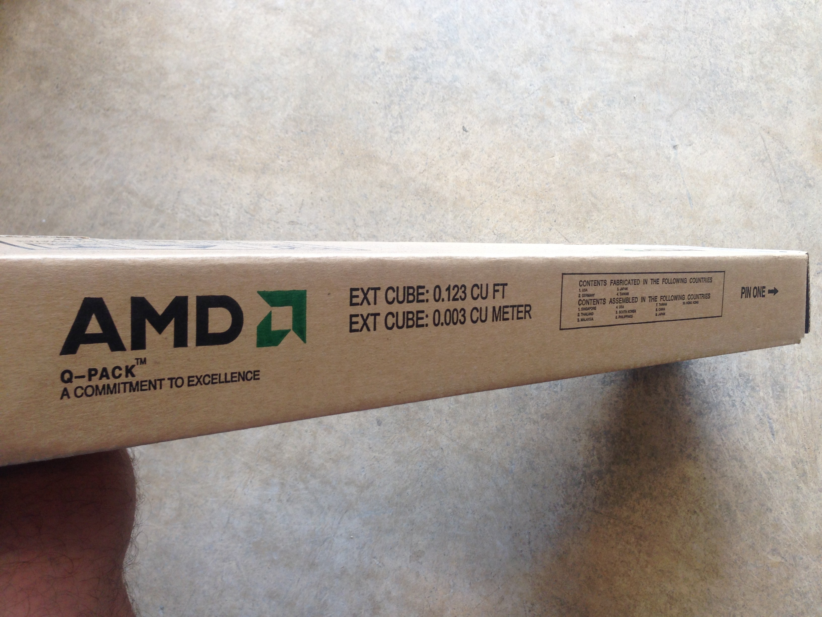
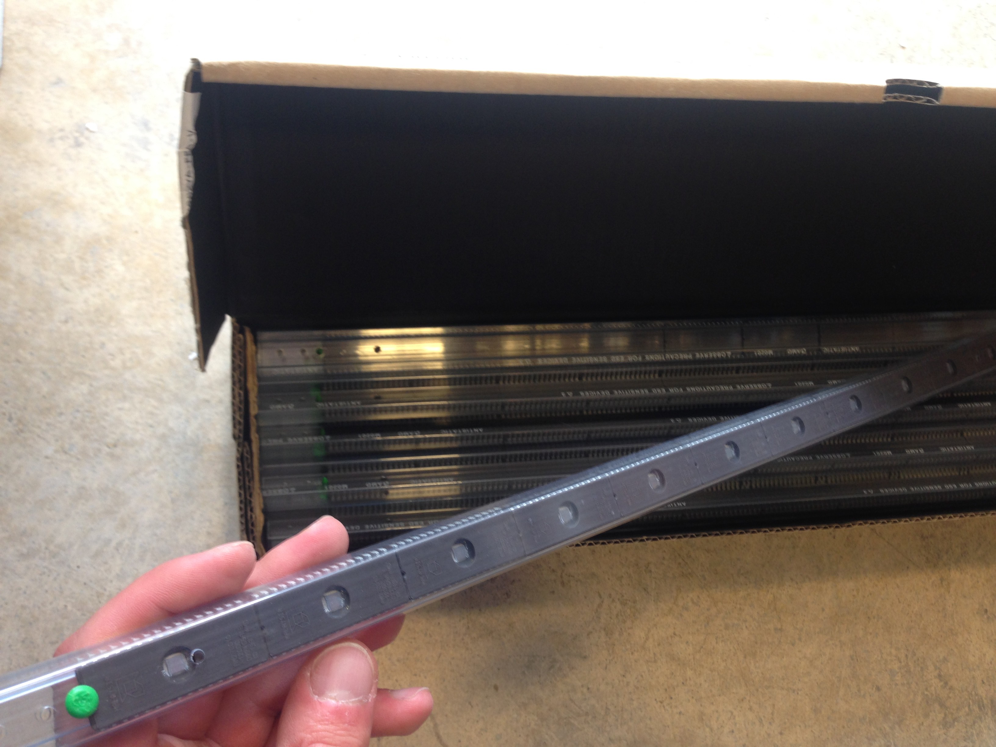
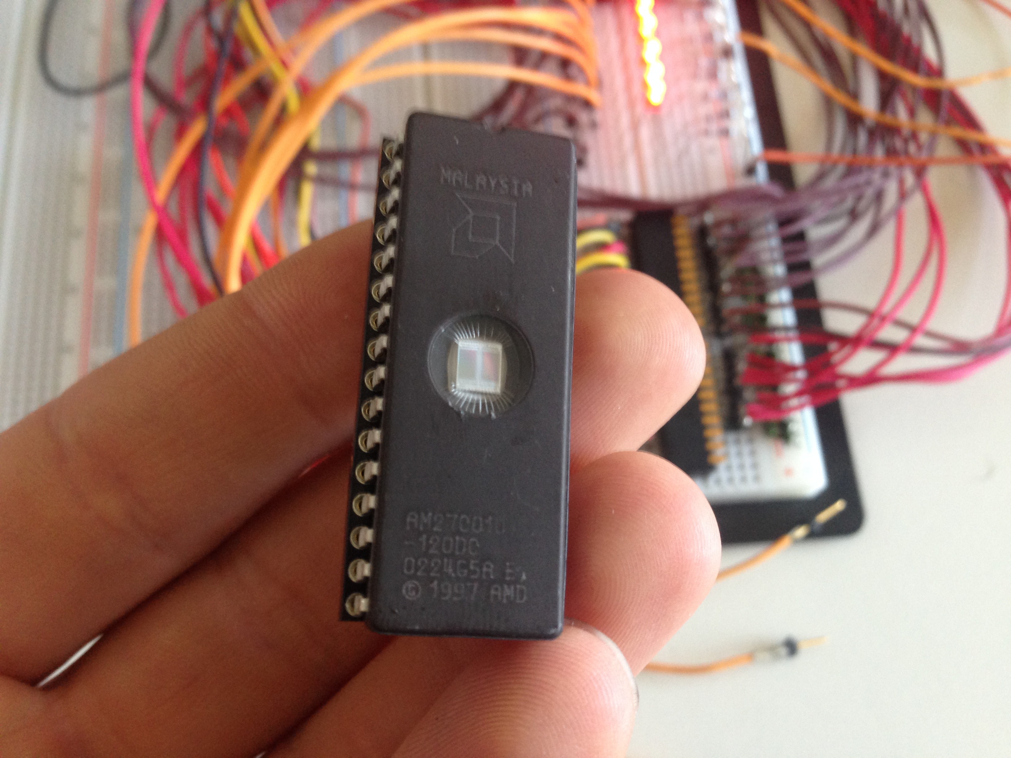
In order to build the memory-card, we need EPROMs. In most cases those EPROMs are UV-EPROMs, or EEPROMs, which stands for electrically erasable/programmable read only memory. In case of UV-EPROM, ultaviolet based erasable/programmable read only memory. Which means, the EPROM can be programmed once, but then needs an ultraviolet erasable device to clear the memory for further usage. This is not as convenient as the first one, but still quite easy to handle. One can buy such devices in electronics shops. Those EPROM's are very fast and mostly handle access times of at about 45 ns. Ideally suitable for micro-controller fast read/write cycles. They utilize the parallel interface which do require some amount of GPIO of the microprocessor. In my case, as one can see from pictures above, I have plenty of those AMD CMOS UV-EPROMs available brand new. So its suits perfect for creating memory card, where several of those IC's can rest, and thus making ideal solution for bigger memory projects without SPI or other types of memory cards and hassle and complexity which they do bring with them.Beside the CMOS EPROMs, a copper/epoxy based prototyping board is need, size may vary depending on how many of the EPROM's one plans to embed. The higher the number, the better for capacity. Next thing would be (green) smd LEDs, and one tht LED (red). Low power, low current (c.a. 20mA) should be fine. One needs resistors for each of those led's (R=150-180 Ohm) for smd leds and (R=470 Ohm) for tht led will do the work. For more convinience I recommend using headers to male the hole card plug-able module, (on solder-less breadboards or anywhere else), size of the headers also depend on the amount of embedded IC's. Jumper wires are needed if you plan to connect them by hand and not on PCB. Each CMOS EPROM require 16 x 10KOhm resistors for address bus data lines and 8x 10 KOhm for data-bus data lines.Each AMD EPROM has 8 ports for data lines and 17 for address lines. So a lot of jumper wires should be available.
Step 2: Assembly Process in Several Steps....
The assembly starts by checking that all the EPROMs are erased and empty.
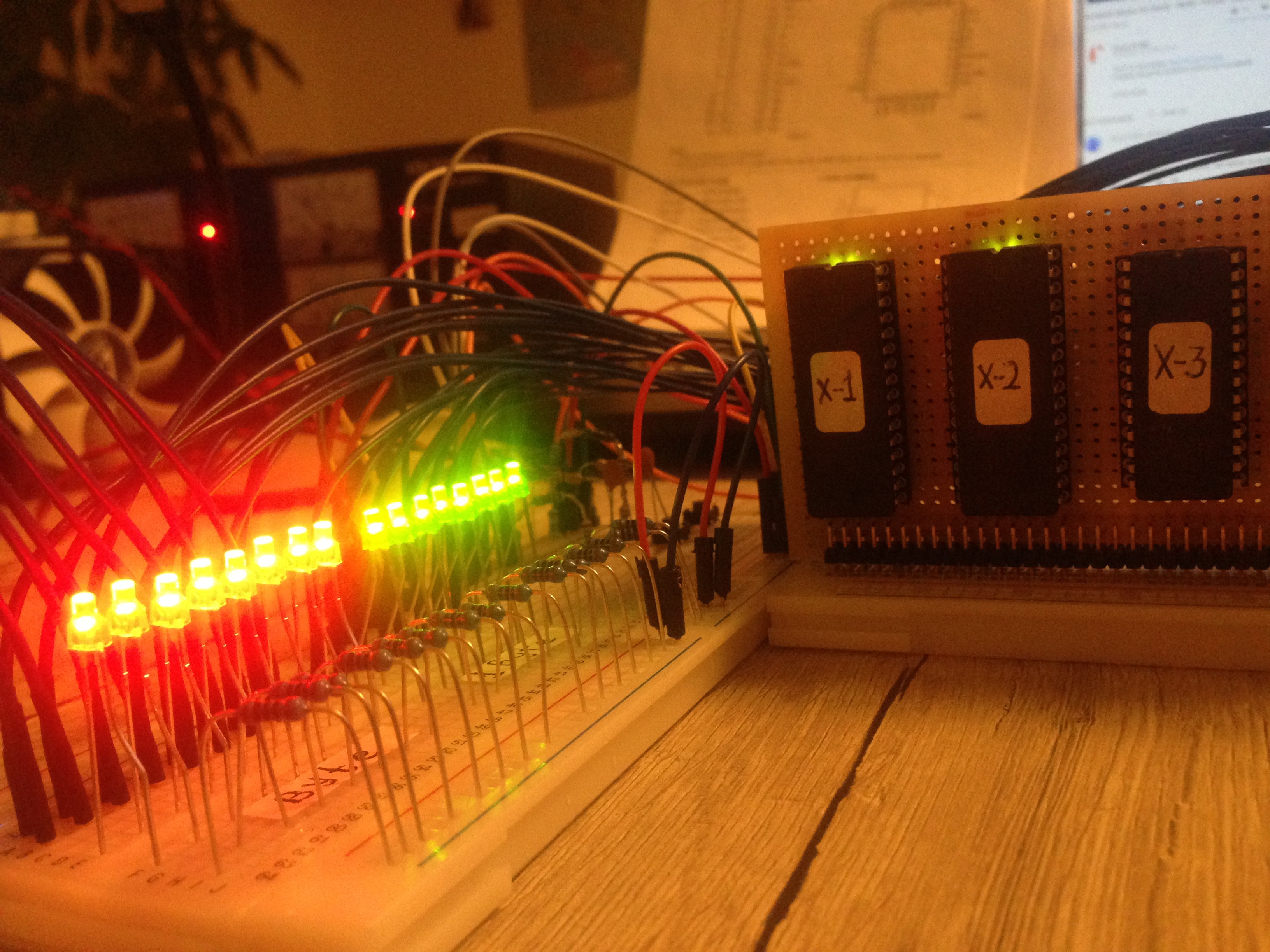
>>Step No0.>> Start soldering a power-bus (+/-) 5.0 V for the entire memory card breadboard. This will help to bring the juice to each IC.
>>Step No1.>> Calculating the space for IC's to be installed, in my case 4 x EPROMs are embedded, with insertion adapters DIP package. This adapters are soldered to breadboard, not EPROMs, which will help you to replace them in case of faults, and or other maintenance works, without hassle.
>>Step No2. >>Soldering the adapters to breadboard, then checking the power-bus rail and connecting the green smd-LED with suitable R=150 Ohm resistor to power rail through the EPROM power-bus. That should be done for each embedded EPROM. The aim is to have power running through led to EPROM, so that one can see visually status of each IC.
>>Step No3. >>On breadboard on lower right corner, a tht red-led with suitable R= 470 Ohm resistor should be soldered. It must be connected directly to breadboard's power-bus, or barrel connector, to ensure that the memory card is powered-up and running (when led is on system powered).
>>Step No4. >> In this step we need to connect each EPROM's 17x address-bus data lines to Ground GND with R= 10 KOhm resistors. Pull them down, in case that we are not used by CPU.On the other hand we need the same 17 address-bus data-lines connect to GPIO on CPU, 17 x GPIO dedicated pins, to enable the address read/write cycles. The 8 bit data-bus data lines are connected to digital pins on CPU (bi-directional) 8 x GPIO. Also one can additionally add 8 x LEDs with R=470 Ohm just to have a binary display, I find its very helpful for learning and or troubleshooting purposes. The 8 data-bus data lines can be shared and interconnected for all EPROMs, In my prototype I did 2x2, with 2 binary displays green, and red, but one can connect all of them to same pins, up to convenience.
Step 3: Control GPIO and Cheetsheet......
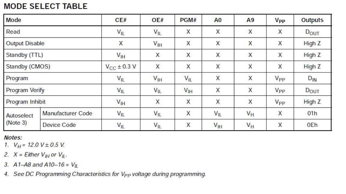
Besides the address-bus data-line, data-bus data-lines and power-bus, each EPROM has control-bus GPIO. Those ones are used for enabling read/write cycles and access to each EPROM, as well as programming them and turning on/off, entering low-power modes etc..... those ports are:
1. PGM-program enable input
2. OE-output enable
3. CE-chip enable
4. Vpp-Program voltage input
Those pins should have dedicated GPIO besides all the address/data GPIO. I highly recommend reading the datasheet and having some idea how the EPROM functions before starting to build the memory card. It will help you understand mostly everything with respect to functionality, programming. part No: AM 27C010 1-Megabit, CMOS EPROM/UV-EPROM.
This table will help you to control the functionality, lets say, if we want to write to EPROM which is same as program, we lookup on table what we need to activate: That is CE=LOW, OE=HIGH, PGM=LOW, Vpp=Vpp=12,75 Volt only for programming... particular address line which we want to program should be HIGH, all other address lines = LOW .
Data-bus meanwhile has to be configured as outputs, in order to output the needed data through the 8-bit data-bus. Simple PIN reading procedure can be used.
In two words: we give Vpp=12,75 program voltage to Vpp pin, then pull down both CE and OE, PGM, after that we put data on CPU data-bus , by pulling the needed address HIGH the EPROM will save the mentioned data at that address. Easy as that. For reading the data from the EPROM, one should refer to that table again, and check what status should those GPIOs be in order to commence other procedures, reading from it, or letting the EPROM go into low power mode. (Standby).
Step 4: Programming the EPROMs

At this point when all the hardware setup is done, and everything is double checked, one can proceed to the next stage.
After going through all the stages above, we can easily start the programming of the memory card, as many times as we want, saving tons of data in each address. Also would be possible to read data from any random address.
There is suitable code (send me pm if code is of interest) together with this device.It very simple one.It will guide maker and help him understand how to program such devices and how everything works. The code configures the suitable GPIO on CPU and then using simple commands runs through every address and writes data there.....if the binary display is connected then, one can see the data output through that LEDs.It will look like a bar which will start fully lit up and then will gradually decrease when the CPU reads through each address.
Step 5: Summery.....
After all the steps we went through, when the memory-card is ready and powered-on, and the EPROMs are correctly configured, all the LEDs on the binary display will lit-up. Also, if we purge the contents of the EPROMs into serial monitor, it will all be 1, 1111111 meaning that all the led are on. That means EPROMs are empty and factory erased with all 1's.
Step 6: Ready to Accept Data...
Now it is possible to program it with the microprocessor, and use the device as external memory module.
At this point you can integrate it into your projects... and benefit from parallel interface speed combined with speed coming so cheap..(^_^). Anyway, I hope someone will find it useful.