 greg davill
At my day job a few years ago I designed a reasonable small product that attaches to the back of a FLIR Tau2 thermal camera core. The product takes the digital video stream from the camera and saves this information to an SD card, it also included an ethernet 100MB/s interface. Since the Tau2 is a small camera, so the electronics in this product is made up of a "stack" of boards.
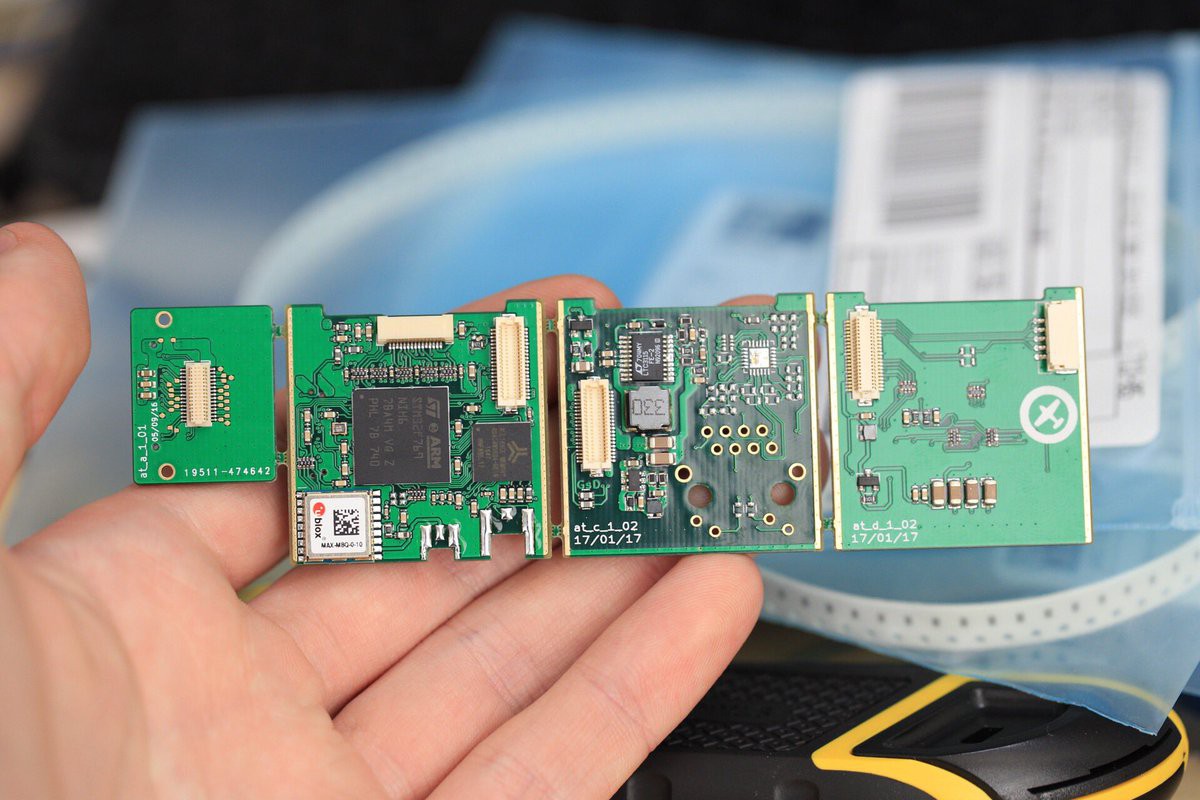
The Tau2 outputs a 14bit video stream of it's 640x512 pixel array. This stream needs to handle upto 60Hz on some product variants, so it features a 27MHz pixel clock. In order to ensure a frame from the camera was successfully captured I designed in enough memory to fully buffer a frame (> 640kb). It's design was based around an ARM M7 microcontroller. Utilizing external DDR memory and it's included 14bit Digital Camera Module Interface (DCMI).
At the time I knew this was the perfect application for an FPGA, but having no hands on experience with them I decided it was too risky at the time.
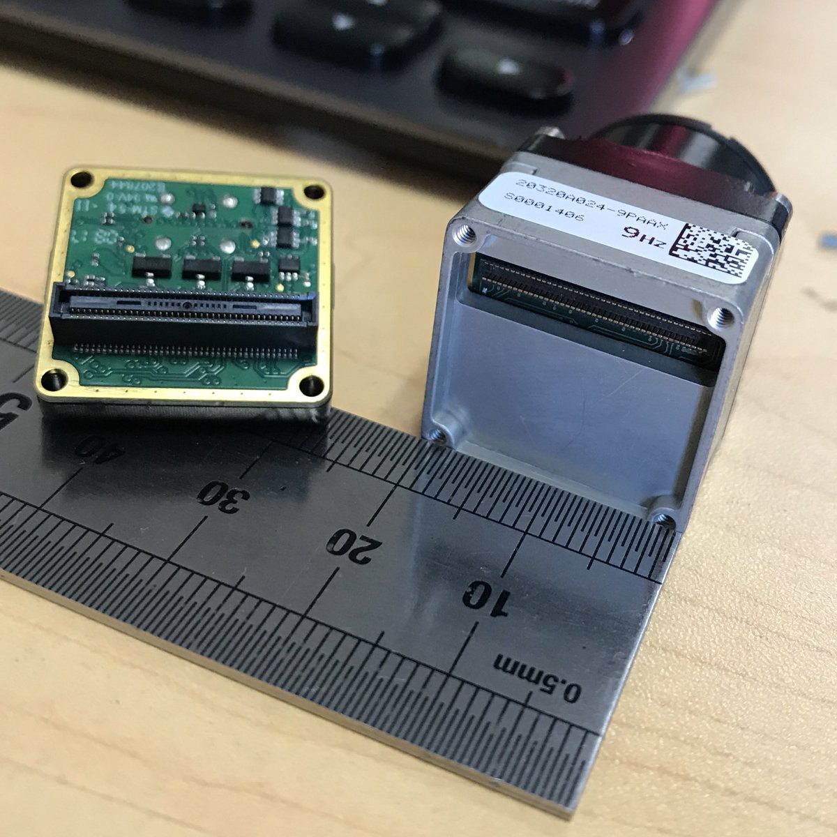
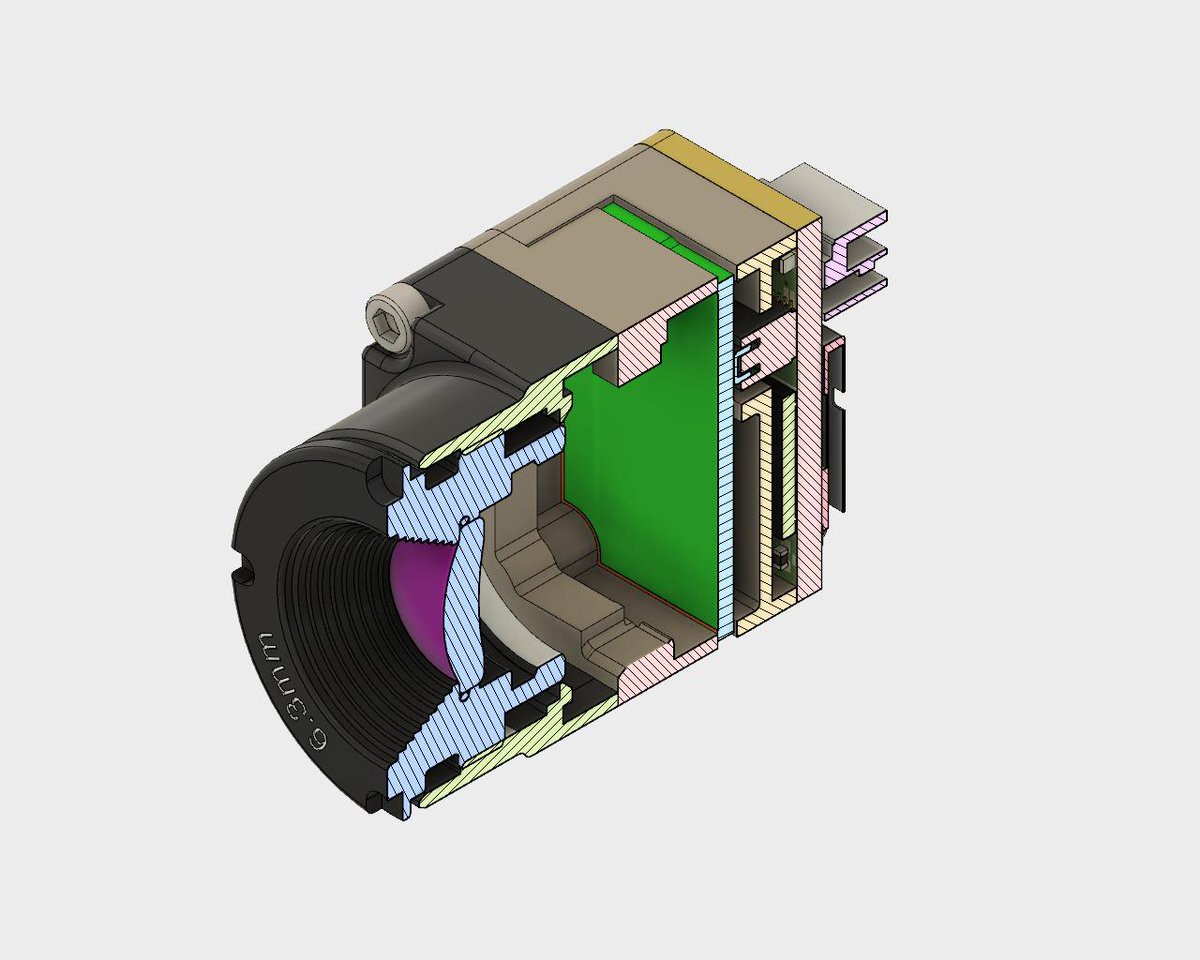
Fast forward to Jan 2018. Our local FLIR rep had loaned us a FLIR Boson 320. The FLIR Boson is a tiny Thermal Camera core. Available in two variants: 320 and 640. These have an image size of 320x256, 640x512 respectively. When I say small, the footprint of the module is 21x21mm!!
FLIR made a nice choice with the interfaces, the Boson supports a USB UVC mode, which enable it stream digital video over USB natively. It also has a 16bit digital video bus, and Analog output. FLIR sells the USB module as "Back" for the camera. Which connects to it's 80pin interface connector.
As a bit of a challenge I decided to teach myself FPGAs with a hands on project. The goal, a small FPGA board that could capture frames from the 16bit camera interface and save these to an SD card. I'd only had experience with FPGAs in a class at university, that certainly gave me a solid understanding of fundamentals, but I'd never actually built an entire project with an FPGA before, how hard could it be?
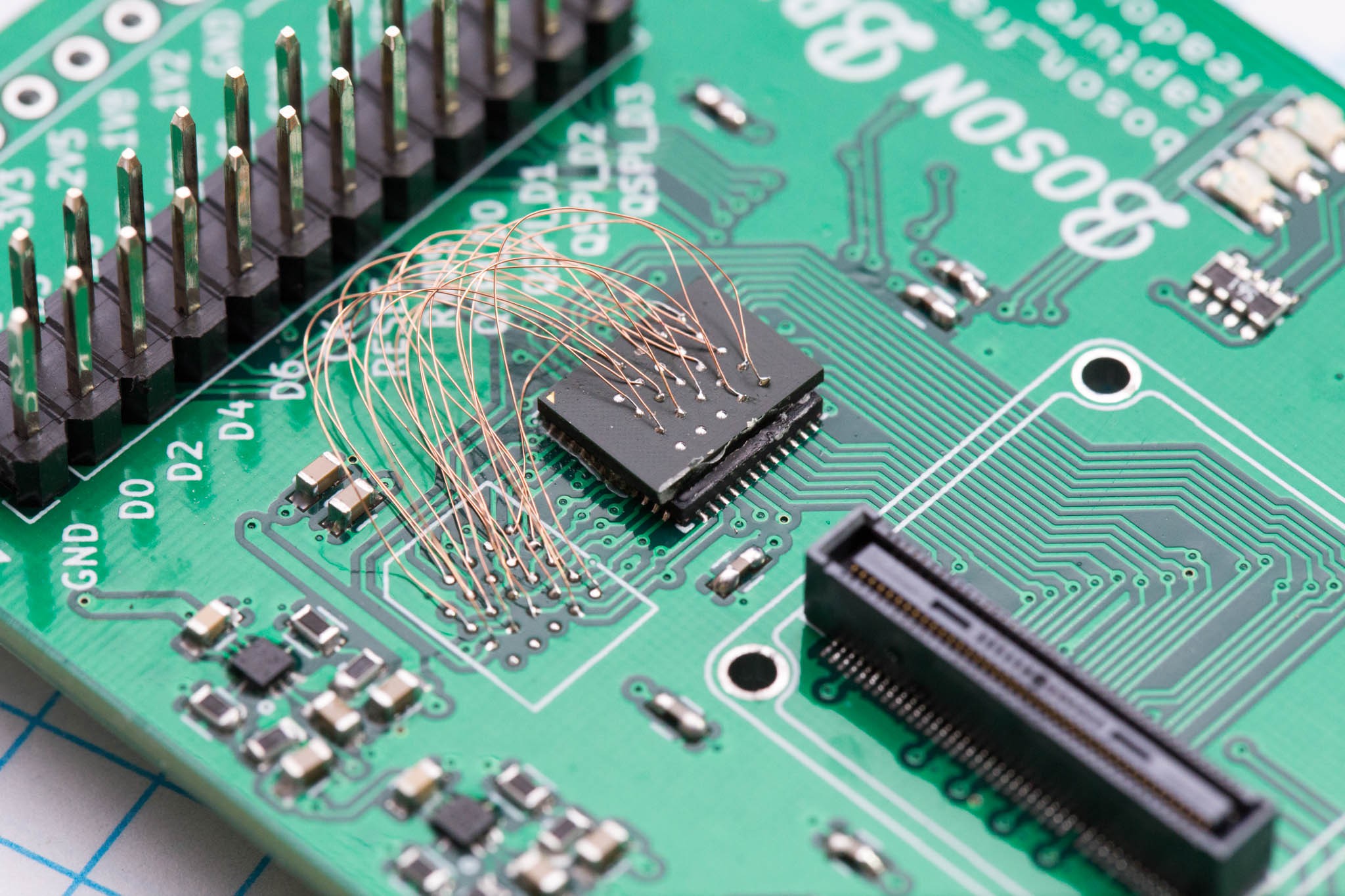
My first idea was to create a hybrid, FPGA/MCU device. The FPGA would be responsible for capturing the fast asynchronous data from the camera storing it external RAM. Then a standard micro-controller could read this data and save it to an SD card. I called this attempt the "Boson Breakout".
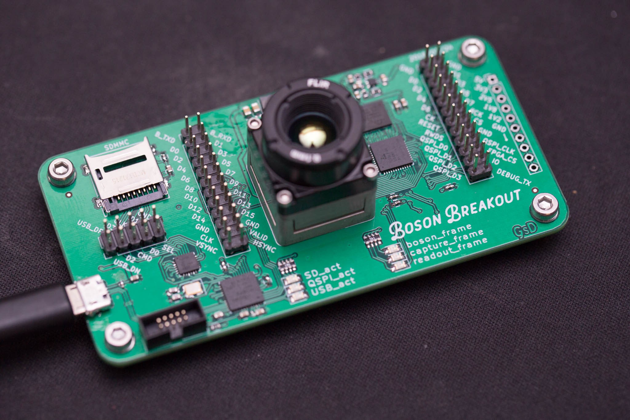
Unfortunately this board never really worked, the firmware remains unfinished. The concept SHOULD work, but there are too many bits and pieces. I also got the footprint wrong on the RAM. ouch.
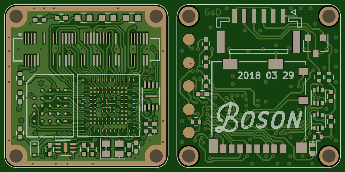
Parallel to "Boson Breakout", I had been researching project icestorm. An open source tool chain for Lattice FPGAs. I unfortunately had used a non-supported Lattice FPGA on my Boson Breakout. Which looking through the offerings of FPGA packages I found the perfect part! The Lattice iCE40HX8K in a 8x8mm package! Combined with a 8Mbit HyperRAM 6x8mm, I might be able to fit everything BEHIND the Boson camera....
After a late night inside KiCad I had this design. A project was afoot!
Discussions
Become a Hackaday.io Member
Create an account to leave a comment. Already have an account? Log In.
I think that it's important to set goals in projects, personal development, and even life. Each job interview questions where you see yourself in 2, 5, 10 years. And sometimes, it's tough to answer it. I've found https://gradesfixer.com/free-essay-examples/where-do-you-see-yourself-in-10-years/ with awesome samples on that topic. To my mind, it's easier to plan your personal development with some examples. Moreover, it's beneficial.
Are you sure? yes | no