 greg davill
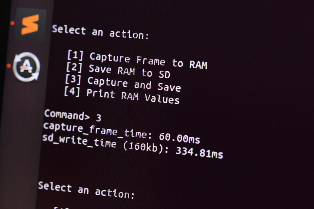
With v1_01 working. I now had a better understanding of working with verilog, and a much better understanding of LUT utilization and timing closure. I'd managed to fit in a hardware SPI module, with DMA. with these improvement and the system running at 24MHz (max frequency of my design typically sat around 30MHz for the iCE40HX) the 160Kb images from the camera took around 300ms to capture. Not bad!
But the iCE40HX8K, while a great little chip is too small and under powered to really push this project to the next level. I had designed the PCB to accommodate a 4bit SD interface, I had wired CMD,DAT0-3,CLK to the FPGA. Using SPI mode was easy to validate that the hardware was working. But for a notable performance increase I'd need to switch to a real SD controller. The controller I wanted to work with (https://github.com/mczerski/SD-card-controller) did not fit in the remaining space of the iCE40HX8K.
Around this time I was contacted by GroupGets. a distributor of the FLIR Boson. They were very impressed with the work I was sharing on twitter, and donated a Boson 640 for me to test with and ensure everything worked.
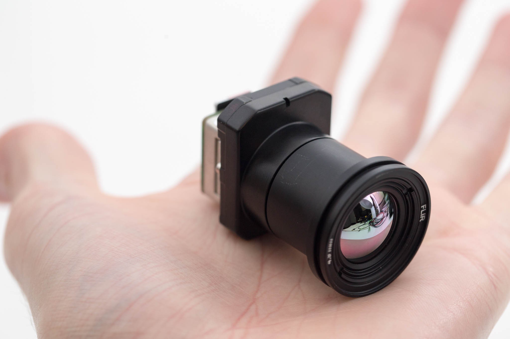
This Boson 640 is a beast! 640x512 pixel resolution, 60Hz update rate, and this has the widest angle lens: 95 degree FOV.
Unfortunately the added pixels (4x an many!) and the added frame rate means this camera uses a 27MHz pixel clock. This did not play well with my 24MHz capture hardware. I needed to rebuild it. Better, faster....(stronger?)
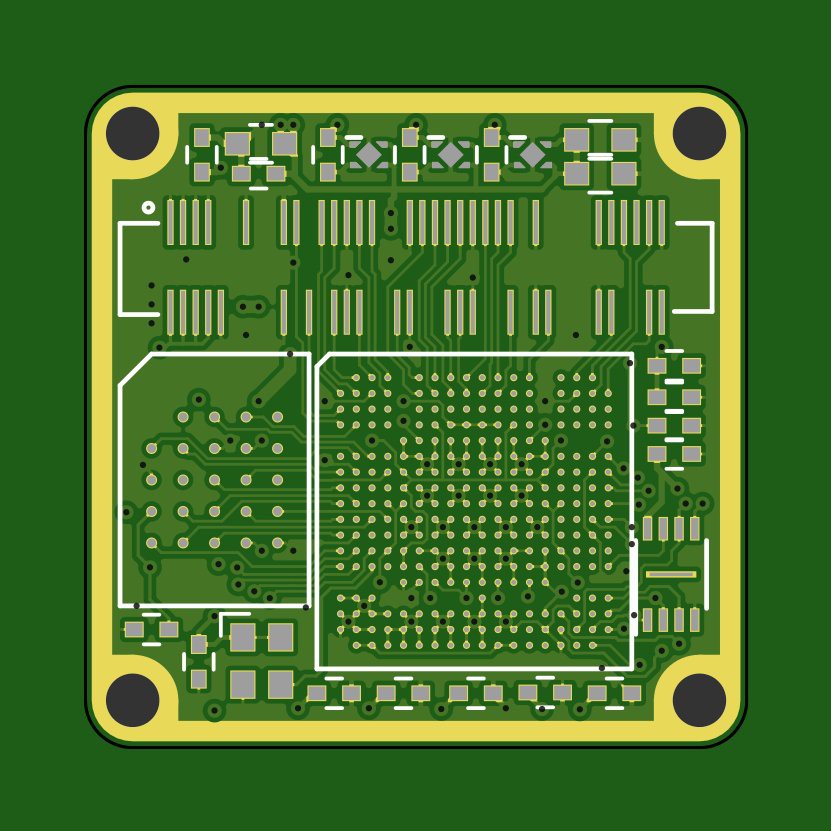
Replacing the HX8k was not easy. Most FPGAs are in huge BGA packages, the ones in small packages typically only have a handful of logic for simple glue logic in modern portable tech. I was very comfortable with Lattice at this point, and finally found the ECP5 line had a 10x10mm package version. While a bit bigger than the HX8K's 8x8mm it might just fit. So I created a footprint and added to my board in KiCad.
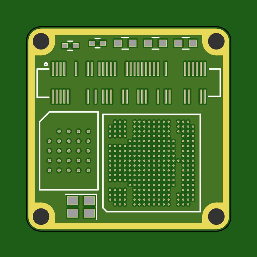
At this point I knew this MIGHT just work. I was not looking forward to prototyping a PCB that required a HDI PCB. But luckily it is possible to route out the connections required on a "basic" 3.5/3.5 0.2mm drill PCB process. This is due to the fact that the majority of the 285 balls in the center of the device are grounds.
It's not super pretty, but it should work. I did have a little trouble with JLCPCB accepting these files, initially they rejected the board. And I couldn't manage to explain to the support engineer that my project did in-fact meet the specifications set out on their website. I submitted the same design again, but also started to rework the design to improve clearances. Strangely they accepted the files without an issue the second time around. (I've since heard this is quite common)
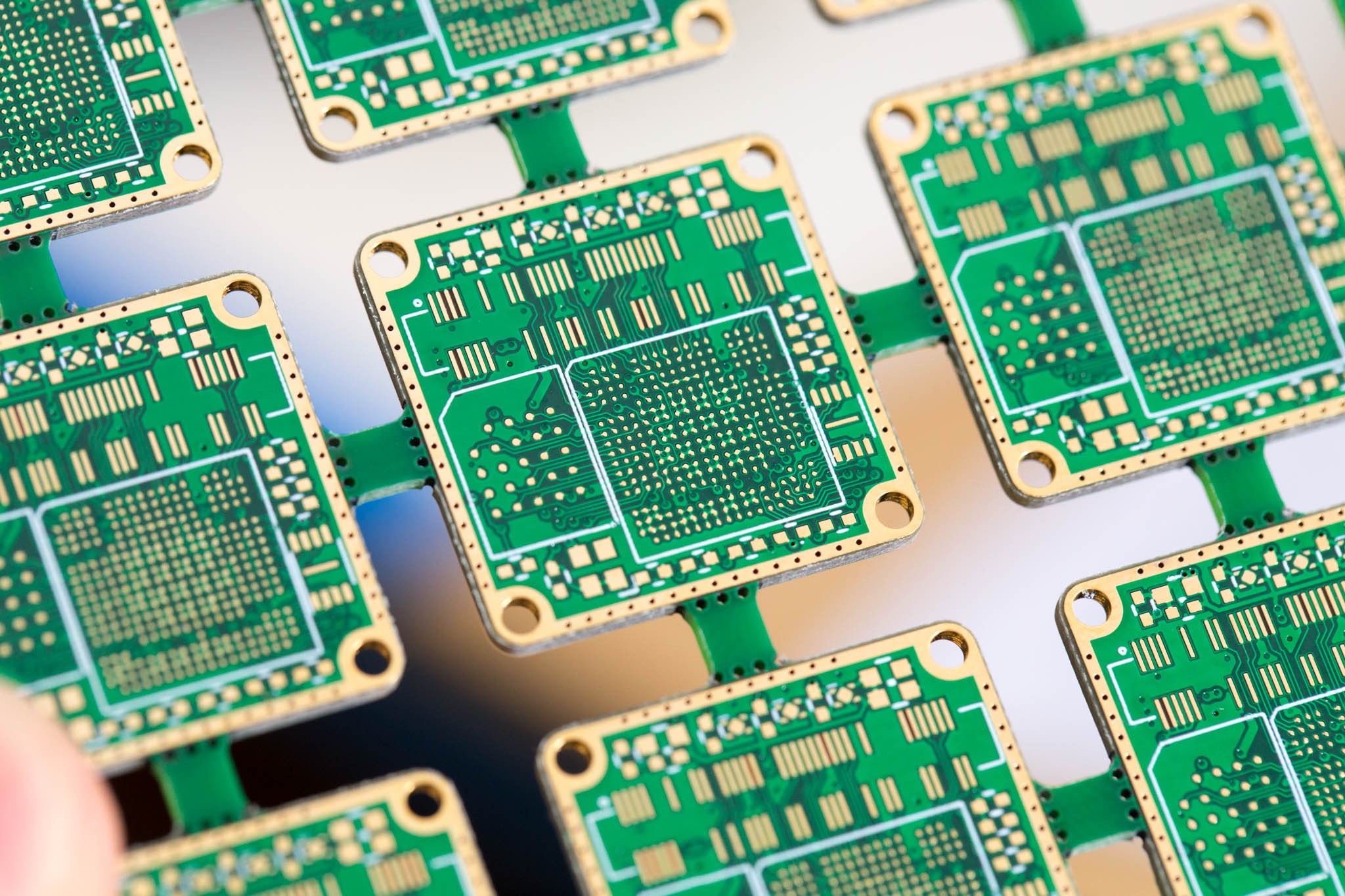 The panels came back looking great! I'm panelising because the design is so small, I can fit 9 copies within 100x100mm. Which gets me their special prototyping price. Since the designs are all the same there is no surcharge for doing this. I'm using this paneliser: http://blog.thisisnotrocketscience.nl/projects/pcb-panelizer/
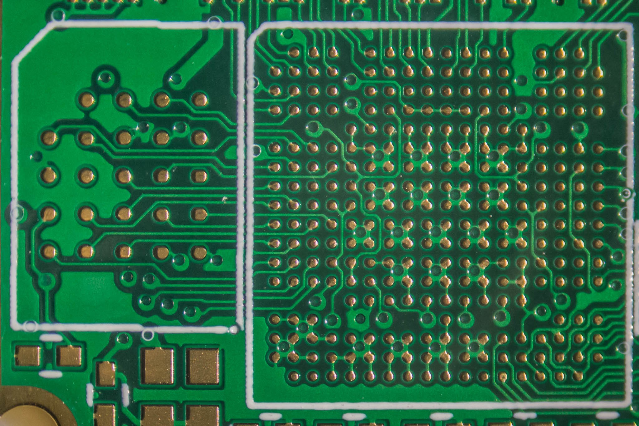
The solder mask registration is slightly off (But still VERY good) these boards should work great for prototypes. If the design works I would be very tempted to try out a board with plugged 0.15mm vias, eurocuircuts lets you cost this up on their online calculator. Since my PCBs are so small the cost per board is actually really good, but there is a steep one time NRE fee.
So far this version of the PCB was going great. With boards in hand I decided to order the BOM and assemble up a prototype.
That's when I found out the cs285 package of the ECP5. The package I needed. Had an 8 week lead time.
Discussions
Become a Hackaday.io Member
Create an account to leave a comment. Already have an account? Log In.