 greg davill
The thought of shelving this project for 8 weeks waiting for the FPGA left me discouraged. What if after 8 weeks I assemble the board and it doesn't work?
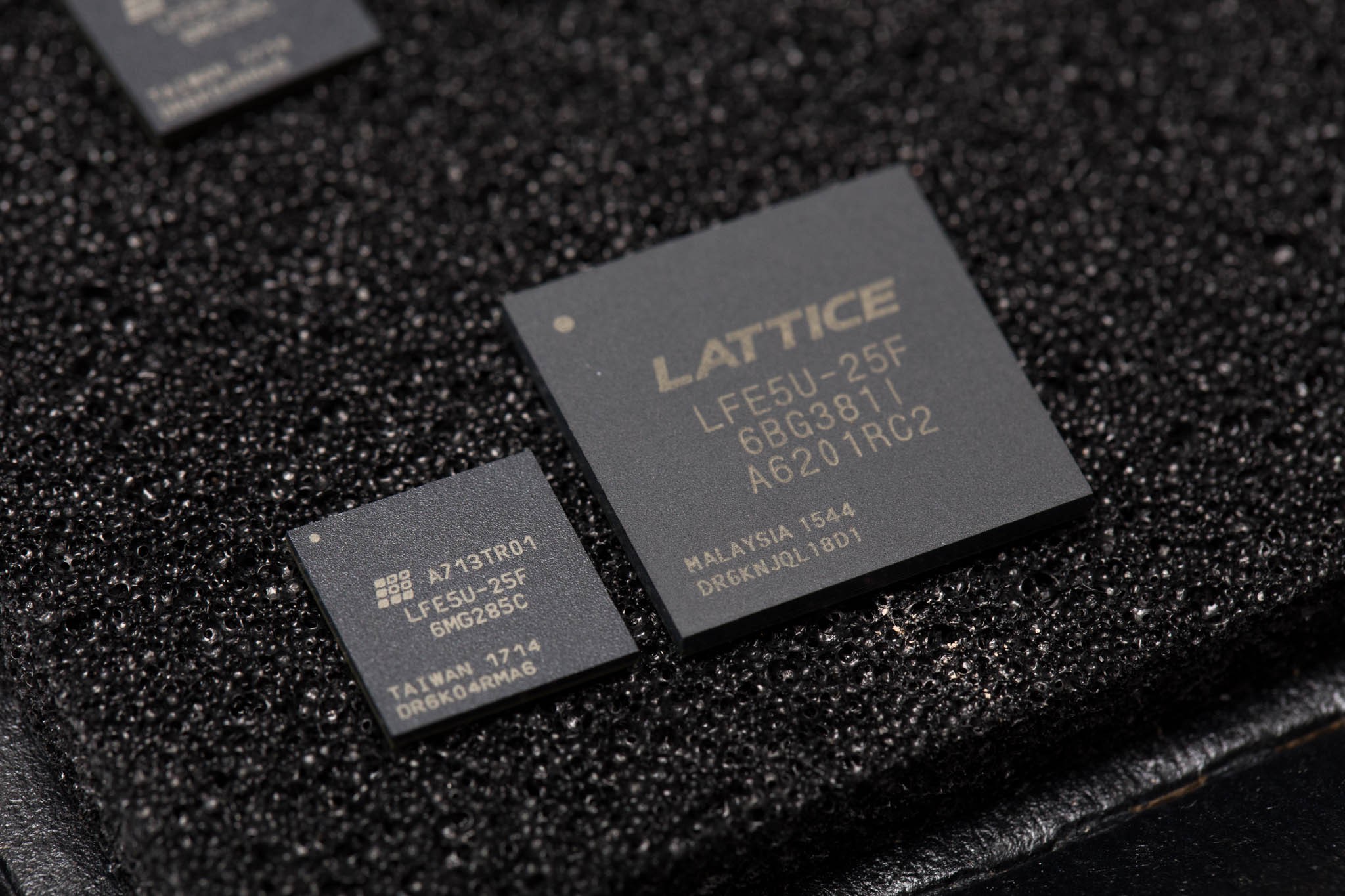
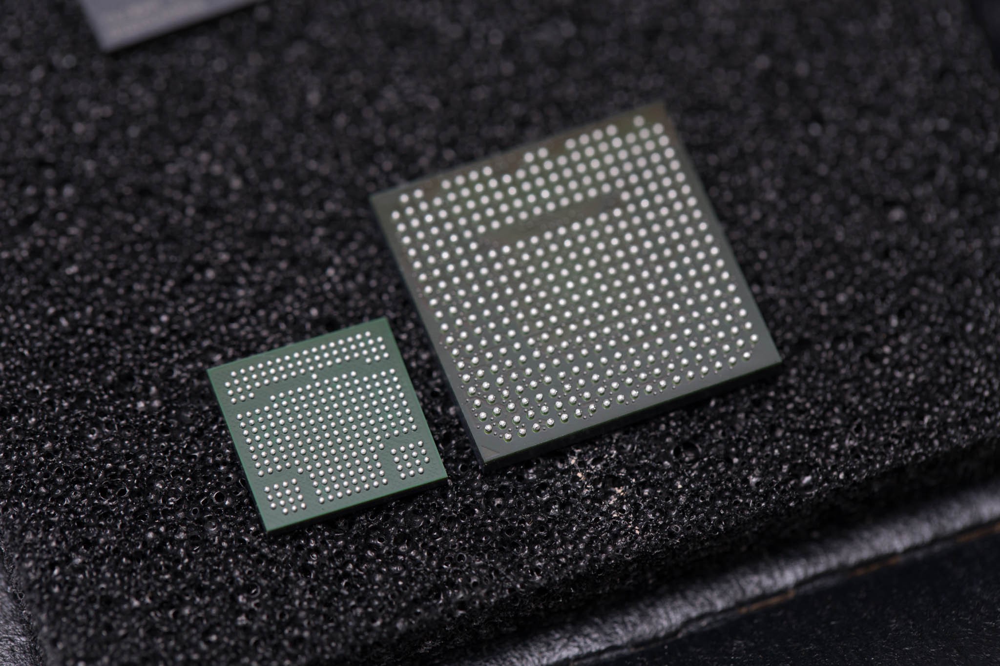
I decided to create a new PCB, this time using an ECP5 in a larger 381 ball (17x17) package.
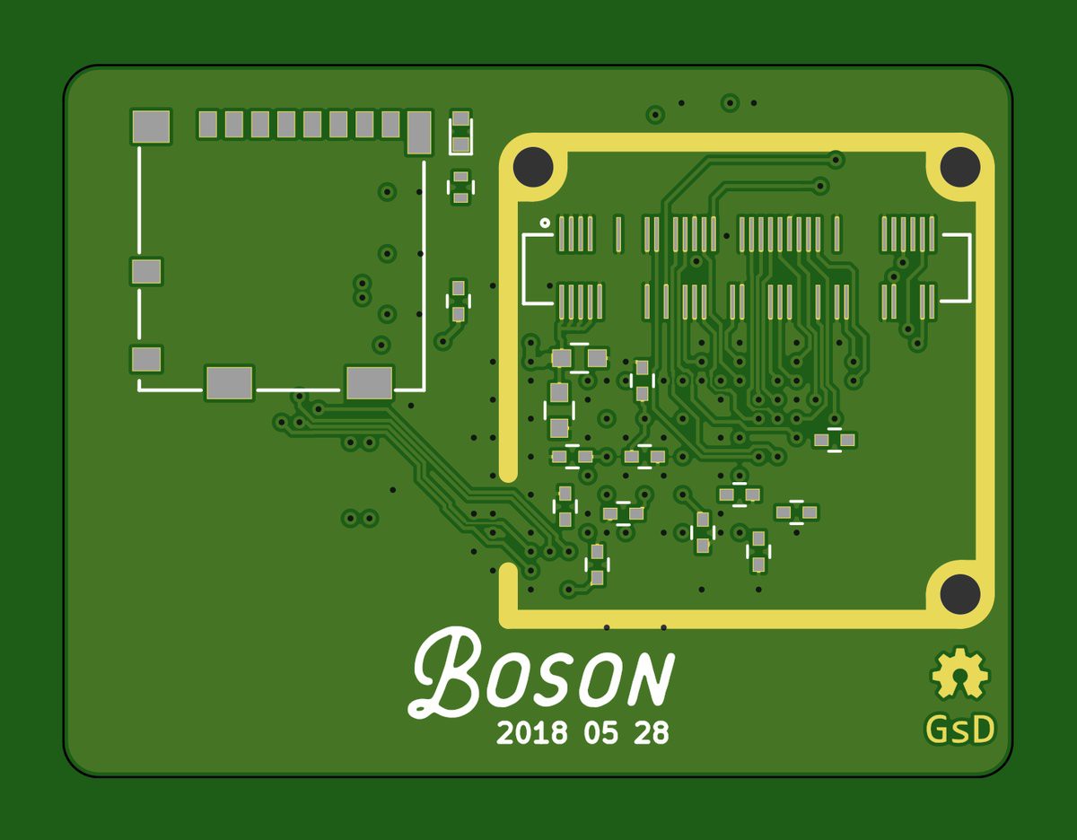
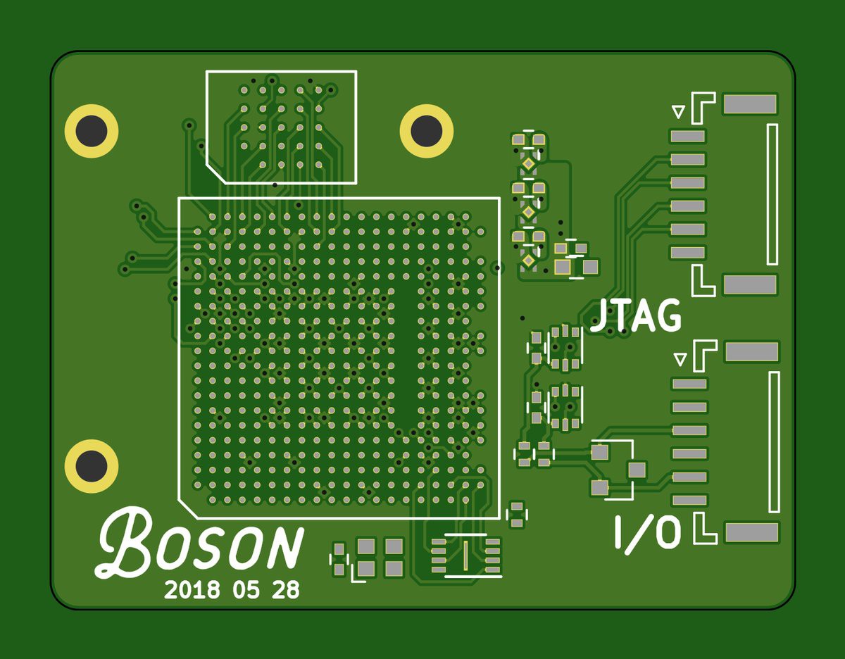
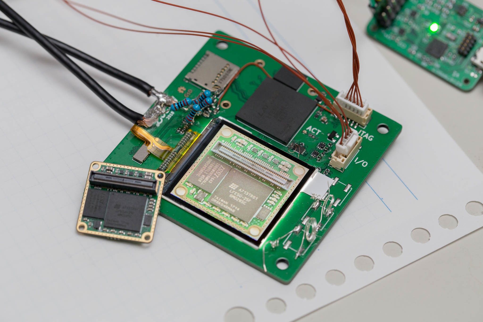
What started as a reasonably small board, soon ballooned as I decide to add an LCD screen. (Why not?)
Unfortunately in the rush to get this board made (I designed it over a weekend) I had introduced a few errors.
- Config flash was not wired up correctly. The ECP5 supports many different configuration methods, and I was not clear in my naming of the signals required in the schematic.
- I had shorted out an internal power rail by adding the via stitching and not running DRC before ordering (rookie mistake) These were fixed by simply drilling out the vias.
- The backlight DCDC circuit for the LCD wasn't connected to a power rail.
- I had incorrectly set the configuration strap pins. so the FPGA would never attempt to load a config bitstream from external flash.
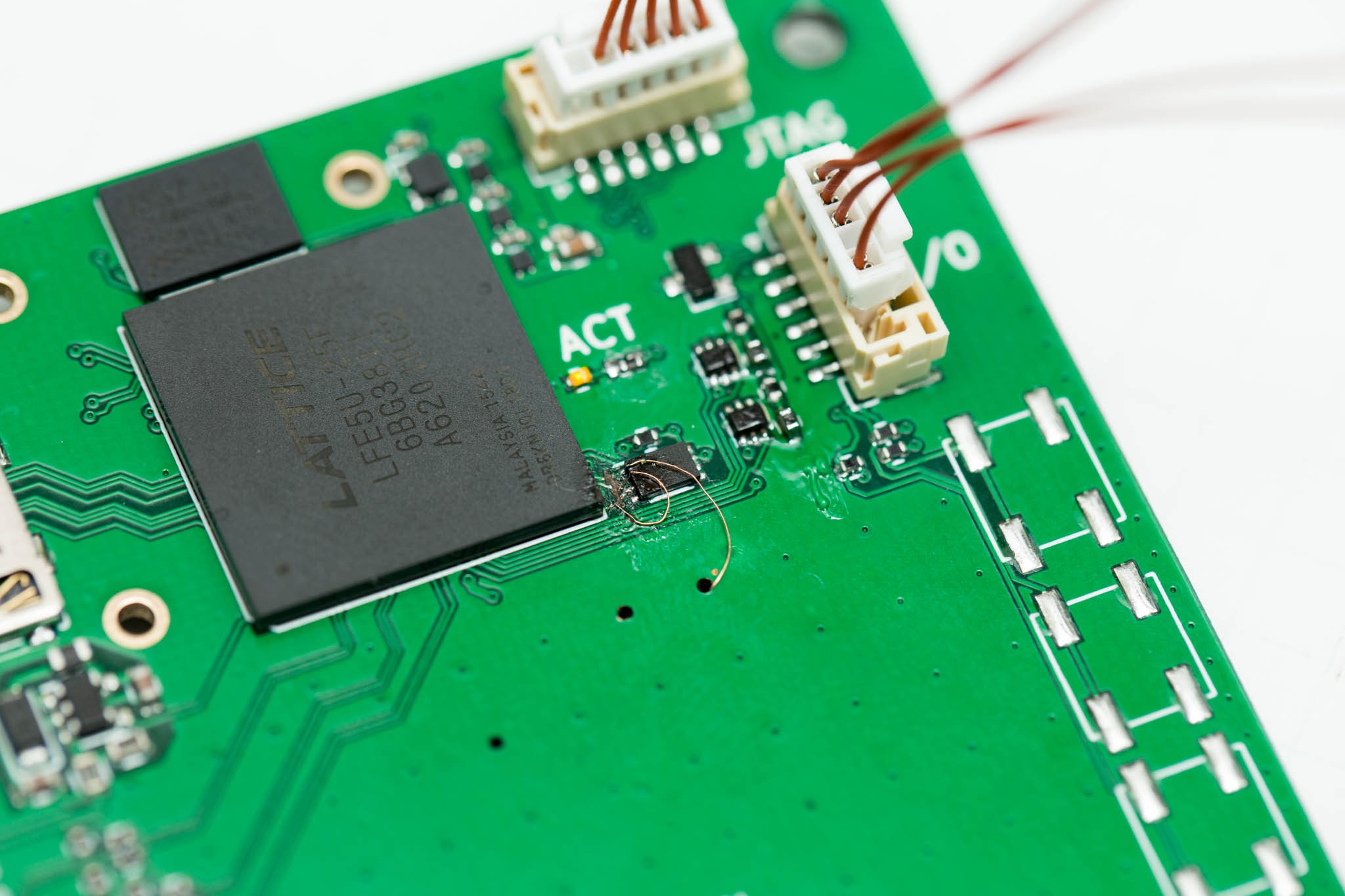
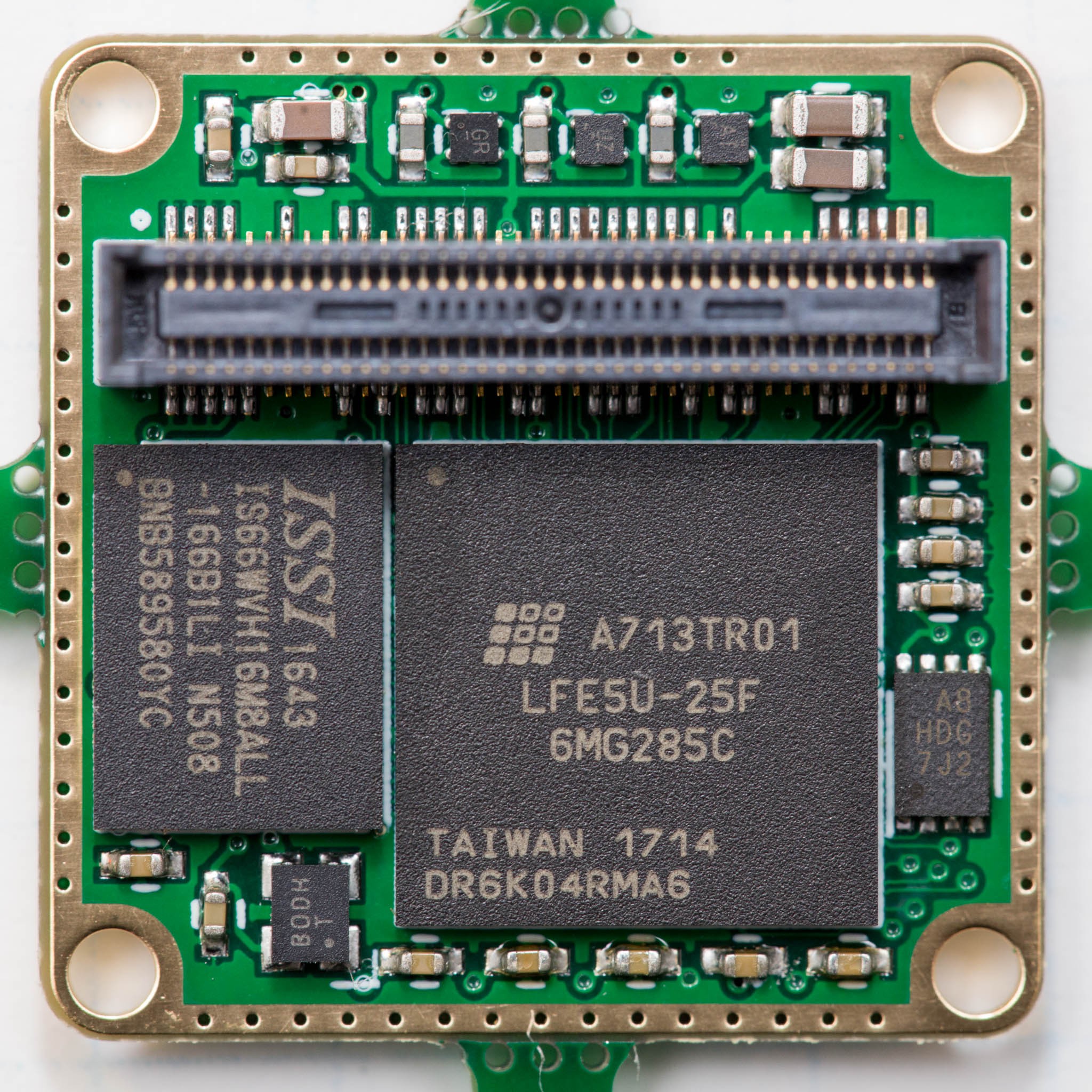
But the good news, I did not make any of these errors on the small boards I already had manufactured. these were all introduced when I swapped my schematic symbols from the 285 pin device to the 381 pin one.
Since I had correctly connected the JTAG pins I was able to program the FPGA after it was powered. So that's something....
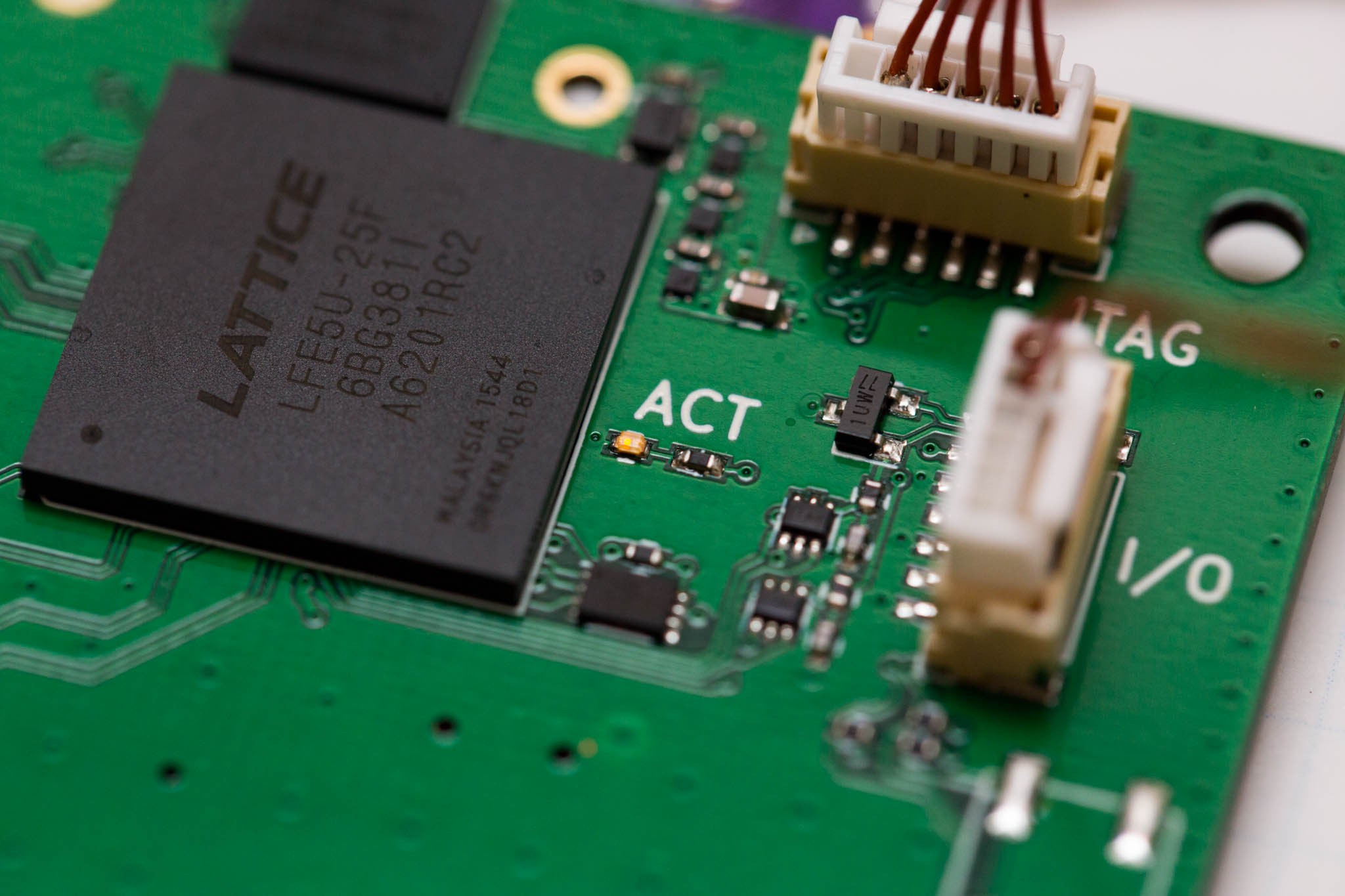
I even did some green-wire fixes to support the FLASH IC. I'm programming the FLASH though the ECP5 in what they call "Background SPI programming". This works great, but does require the FLASH chip be connected to the correct pins on the chip.
While working on this board did keep me busy for 2 weeks, it was all for moot. I'd been checking the lattice webstore for ECP5 stock every couple of days. The day after assembling this larger test board I find they have stock of one product line in the 285 ball package.
Lattice actually uses Mouser as their fulfillment center for their webstore. So I checked Mouser, and yes they had a tray of the FPGAs in stock. I bought a few as spares.
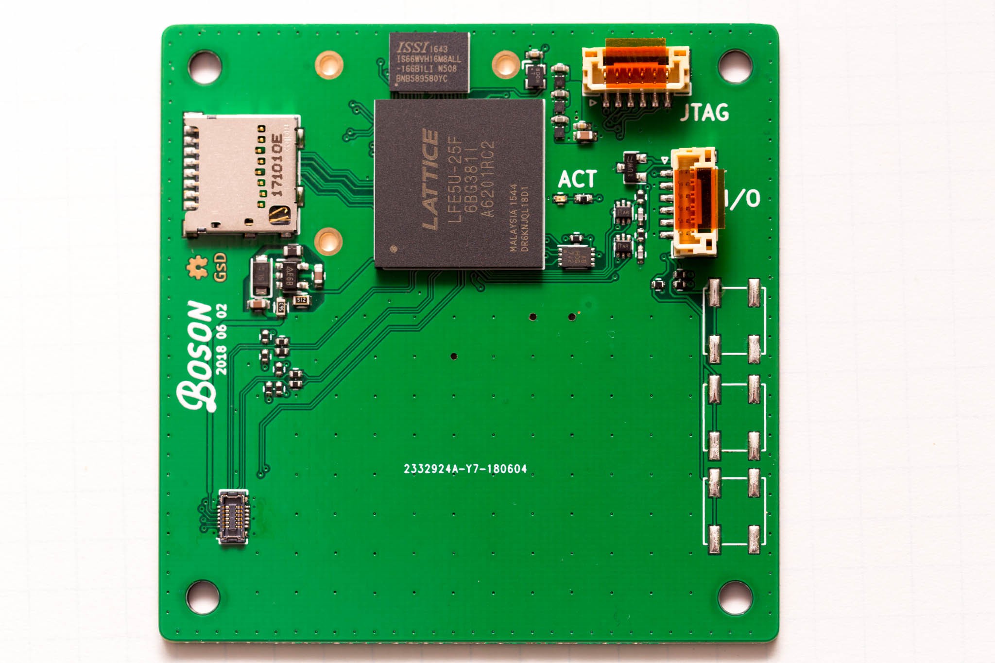
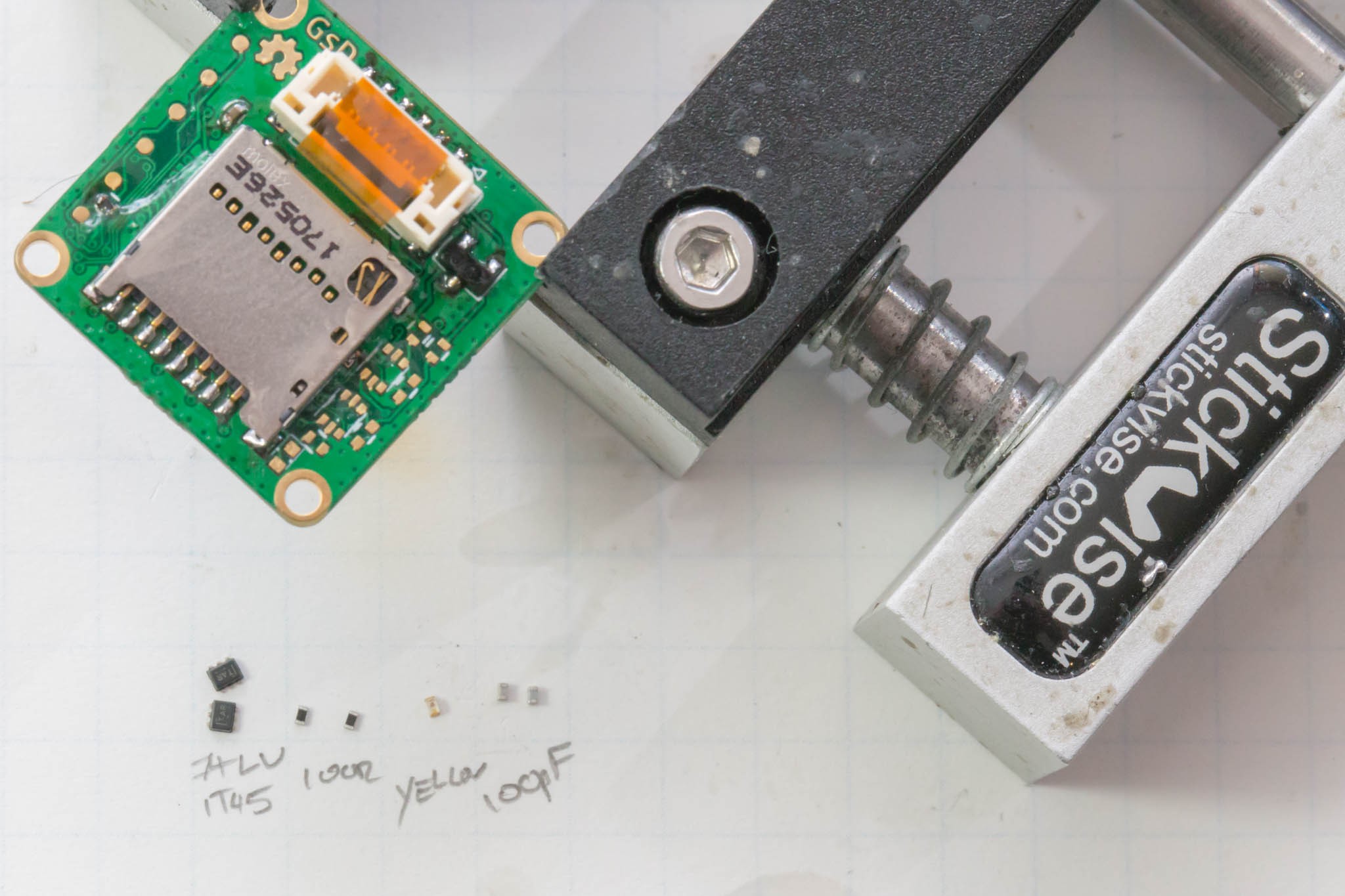
With these FPGAs in my hands I assembled up my first v1_02 PCB. Even though the spacing between parts is very tight, it's actually not too difficult to assemble one of these boards by hand under a microscope. I'm using lead free solderpaste and a stencil (from OSHStencils). The boards are double sided. The reverse side I currently hand-solder. You do have to be careful about the order in which you solder parts as to leave clearance for the iron.
I did end up playing around with that LCD I'd put on the big-board. It's an ipod nano 240x240 IPS panel. Mike Harrison did a great job reverse engineering it (http://www.electricstuff.co.uk/nanohack.html) Following his instructions I manged to replicate the MIPI bus using the ECP5. I even had to make up some x10 low impedance scope probes, which he explains in his very detailed videos.
 I might revisit the big-board and a project with the ECP5 and an LCD screen at a latter date.
Discussions
Become a Hackaday.io Member
Create an account to leave a comment. Already have an account? Log In.