In this log I will explain more about the connections to the CPU.
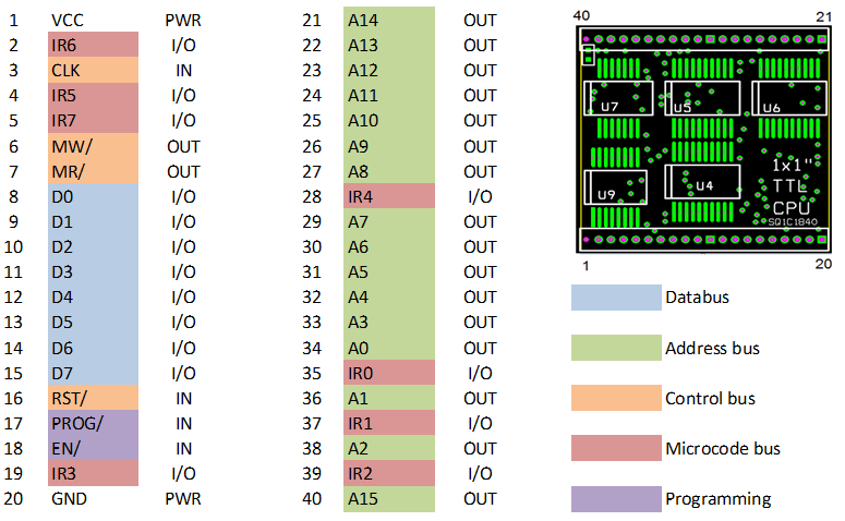
To use the processor, you only need the databus, address bus and control bus to connect memory and I/O to the CPU. PROG/ must be high (inactive) and EN/ must be low (active). Address lines A3 up to A14 need an external 2K2 pull-down resistor.
VCC must be 5 volt. A suitable TTL clock signal must be applied to the CLK input. To start the CPU, the RST/ signal must be low during one or more clock cycles. After reset, the CPU will fetch its start address from the first ROM bytes at address 0x8000 (lsb) and 0x8001 (msb). Afterwards, instructions can be fetched from any position in the 64K address range.
When the processor makes the MR/ signal low, the selected memory or input device should place a byte on the databus. When the processor makes the MW/ signal low, the databus contents should be written to the selected memory or output location. An external demultiplexer will be needed to select RAM, ROM or I/O.
MICROCODE PROGRAMMING
The microcode bus and Programming signals are needed to program or update the microcode (that is in the flash memory of the CPU). Normally, the microcode bus will output the microcode bits. This can be used for debugging, but it is not needed to connect this for normal operation.
To go to programming mode, stop the clock (make it high). Make EN/ inactive (high) to disable the output of the microprogram memory. An external device can now place a microcode instruction on the microcode bus, and this instruction will be executed by the CPU when there is a low pulse on the clock. This external device can be a RPi (Raspberry Pi), that is used as programmer, in almost the same way as described in This log for the RISC Relay CPU. The web-based Javascript assembler for the One Square Inch CPU will be discussed in another log.
To program a microcode memory location, the correct address must be set in the UPC register, and the flag bit (bit 7 of the H register) must be set correctly. This can be done by letting the RPi send microcode and databus bits to the CPU, to accomplish this. When the correct address has been set, the byte that must be programmed can be placed on the microcode bus, and a short active-low pulse on the PROG/ input will program the byte into the flash memory (the exact programming sequence is a little bit more complicated, refer to the datasheet of the flash device). To check the programmed byte, the EN/ input can made low to read the microcode byte from the flash.
Note that the microcode is non-volatile, once programmed it will always stay in the CPU, also when there is no power.
The programming mode can also be helpful to program the external flash ROM that holds the user program for the CPU. By sending the correct microcode instructions, the address bus can be set to the address that you want to program, so no external multiplexer is needed to connect the programming address to the flash ROM. But of course it is also possible to have the external flash in a socket and program it by inserting it in a universal programmer.
Discussions
Become a Hackaday.io Member
Create an account to leave a comment. Already have an account? Log In.