CPU demo: CLOCK
Since yesterday, the clock application is fully working. It includes button functions for setting the clock to the current time. The browser based Javascript assembler was updated again, it will now show today's clock source code when you open the page.
An "Assembler code manual" was made and put in the files section today.
This log will discuss the pcb that was made for the clock demo.
For the full schematic of the clock application pcb, please refer to the CLK1840.pdf in the files section. The gerber fies are also in the files section.
ADDRESS DECODER
The address decoder on the schematic and pcb is this:

This was designed very quickly before the implications of all design decisions were known. But it has the possibility to swap the address range of ROM and RAM, by leaving R30 and R31 out and cross-connect them. It also shows that when the programming of the application flash is enabled (PR_ENA = 0), the ROM will always be selected. That is needed because for programming the ROM, all 16 address lines must be controllable.
However, this circuit must be changed by modifications on the pcb:
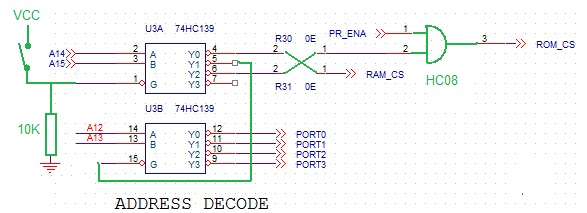
As you can see in other logs of this project, ROM starts at 0x8000 so the R30-R31 swap must be done. And the I/O ports were not properly decoded, that's also corrected here.
The ROM can be selected by the decoder OR by the PR_ENA signal, so at first sight the HC32 OR gate was OK. Just too bad that these signals are active low, so a HC08 AND gate is needed. I soldered it on top of the the HC32 (the outputs not connected), disconnected pin3 of the HC32, and a short piece of wire did the rest.
And during programming of the microcode or application flash, the Raspberry Pi needs control of the databus. That would become a mess if the Flash ROM or RAM of the clock pcb would also put something on the bus. So, during programming, the switch must be closed to disable the ROM and RAM (In my version, the switch is just a wire with crocodile clips). The Raspberry Pi can however still read or write to/from the application Flash ROM because it can enable it by the PR_ENA line.
For a next version, the switch should be a signal controlled by the RPi.
CPU CLOCK
The cpu clock is a free-running RC oscillator built from a schmitt-trigger port HC132:

The clock runs at 440kHz but can run a lot faster, that just hasn't been tried yet. For normal operation, the clock must be running, so PR_ENA must be 1 and PR_CLK must be 1. During flash programming, the clock will be stopped by making PR_ENA high, and the RPi can give single (active-low) clock pulses by making PR_CLK high (will give a low pulse on CLK).
There is a small problem with this circuit. When the CPU is single-stepped by the Raspberry Pi, the PR_ENA must be high (otherwise ROM is enabled all the time, see ADDRESS DECODER). But that means that the clock is not properly stopped. The workaround is, that the timing capacitor C2 must be manually shorted during single stepping. Room for improvement !
REAL TIME CLOCK
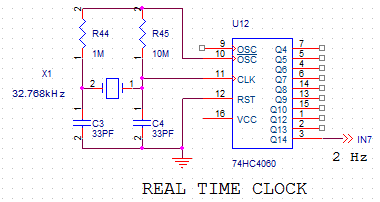
The real time clock delivers a 2 Hz signal derived from a watch crystal. At first it didn't want to run at the correct frequency. It took me some time, but the solution was simple. The power bypass capacitor for the 4060 was not close enough to the chip (a few cm away). After bypassing VCC directly over the chip, with 100nF, it ran perfect (the schematic shows VCC unconnected, but it certainly is connected on the pcb). The 4060 is the only chip that is SMD (SO16) and mounted on the bottom side. All other chips on this pcb are DIP and mounted on top side.
CPU CONNECTION
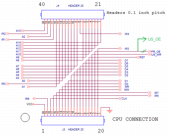
Here you see the connection to the "big" NAC (No-ALU-CPU). Two headers are shown, but they are placed at 0.1" distance to form a 2x20 header. One of the pins was connected to PR_OE instead of US_OE. It was corrected with a wire directly to the US_OE signal on the programming connector, and a trace cut at the right position. The smaller, but identical connections to the 1x1" CPU were wired correctly.
PROGRAMMER CONNECTOR
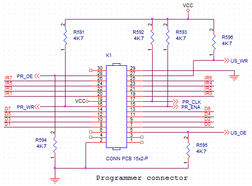
Here you see the connection to the programmer. The interface is the same as the one used for the RISC Relay CPU (even the resistor numbers are the same). A small pcb is between this connector and the Raspberry Pi. The small pcb puts the signals at the right pins, and handles conversion between 5V and 3V3.
There are three groups of control signals:
PR_ENA and PR_CLK let the RPi control the CPU clock. The clock can be disabled, and single clock pulses can be given.
US_OE and US_WR (Microstore-output enable and Microstore-write) are used to disable the output of the microcode flash, and give a write pulse to the microcode flash.
PR_OE and PR_WE are used to disable the output of the application flash, and give a write pulse to the application flash.
Bits IR0 up to IR7 are the datalines for writing the microstore flash. Bits D0 up to D7 are the datalines for writing the application flash.
Note that when the Raspberry Pi is not connected, the control signals have pull-up or pull-down resistors to enable normal operation of the CPU.
DISPLAY OUTPUT
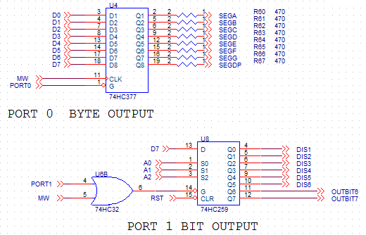
The display output is a standard multiplex system. The six displays are common anode types. Segments are driven by port 0 (0x4000) with 470 Ohms series resistors. The correct digit must be selected by port 1. The IC for port 1 is an addressable latch, that means that the outputs can be written independent from each other, at addresses 0x5000 - 0x5007. The output signals are bit 7 of the databyte that was written.
Note that the outputs are written at the end of the active-low MW pulse. The HC377 has a special input that enables the clock input only when port 0 is selected. The HC259 does not have this, so a HC32 is used, that will only pass the clock when port 1 is selected.
I/O CONNECTOR
The clock pcb can also be used for other applications than a clock ! That's why it has
an I/O connector.
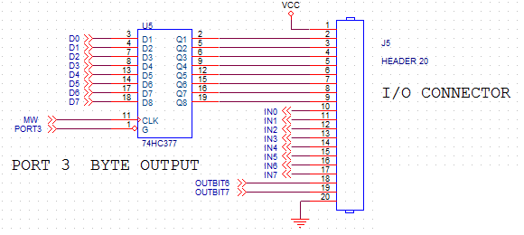
The 20 pin I/O connector has 8 bit-addressable inputs on port 2 (but the IN7 signal can not be used because it is connected to the 2Hz RTC). Three of the other inputs are shared with the three control buttons B4, B5 and B6. The 8 bit-addressable inputs have address 0x6000 - 0x6007. After a read from this port, the input bit lands in bit 7 of the accumulator, so it is easy to test the input state with a BRM or BRP instruction. The inputs have an on-board pullup resistor.
The I/O connector has 2 bit addressable outputs from port 1 (OUTBIT6 and OUTBIT7, 0x5006 and 0x5007). The other 6 addressable outputs are used to enable one of the six 7-segment displays.
It has an 8-bit parallel output (port3 at 0x7000) that is not shared with anything.
Discussions
Become a Hackaday.io Member
Create an account to leave a comment. Already have an account? Log In.