-
JavaScript assembler and simulator
09/23/2018 at 13:45 • 0 commentsThe Online Javascript assembler-simulator from the RISC Relay CPU was changed. It now knows the instructions of the new CPU. It also assembles the microcode (but the source of the microcode is for the moment fixed in the Javascript code). It can simulate the instructions at the microcode level. If you press SAVE, it will store 3 files to your local computer:
- The source code
- The object code in hex
- The microcode in hex
To use it, click One Square Inch CPU assembler and simulator !
Not much testing was done yet, so changes are likely to come. Therefore, I do not post the JS code yet.
[edit: JS code is in the files section now]
-
First PCBs arrived
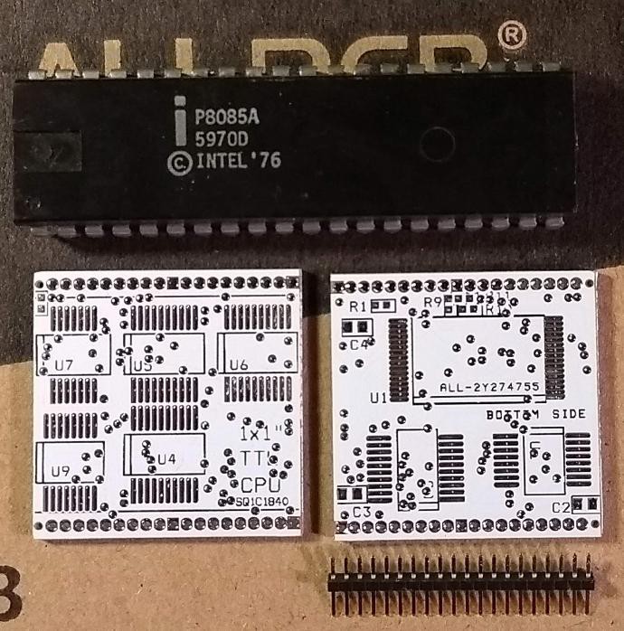
09/21/2018 at 18:05 • 2 commentsTop and bottom side of the square inch PCB. Compare the size to an antique 8085 CPU ! The 1.27 mm header is very tiny, never used that before....
![]()
You might have noticed that the last hole on both the headers has no pad around it. Reason is, that with a pad, the pads would come too close to the border of the PCB, according to the design rules of the PCB manufacturer. So I removed the pad there, but the hole is still there, and the headers are placed a little bit out of center so the pad at the other side has enough space. The pins must be connected to a nearby pad with a small wire. For pin 1 (VCC) this connects to C2 (lower left side on bottom), and for pin 40 it connects to a dummy-resistor very close to it (upper right side on top).
Unfortunately, the bigger support pcb's are delayed, and will come after the weekend...
-
Processor pin description
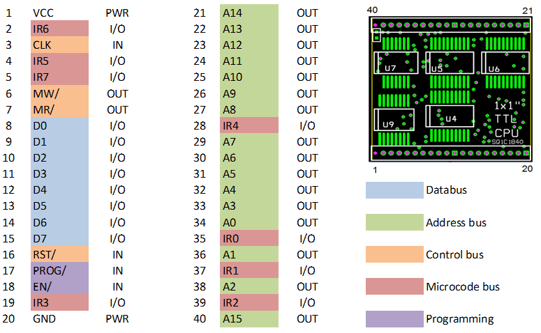
09/21/2018 at 07:59 • 0 commentsIn this log I will explain more about the connections to the CPU.
![]()
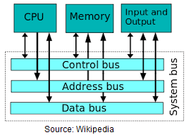
To use the processor, you only need the databus, address bus and control bus to connect memory and I/O to the CPU. PROG/ must be high (inactive) and EN/ must be low (active). Address lines A3 up to A14 need an external 2K2 pull-down resistor.
![]()
VCC must be 5 volt. A suitable TTL clock signal must be applied to the CLK input. To start the CPU, the RST/ signal must be low during one or more clock cycles. After reset, the CPU will fetch its start address from the first ROM bytes at address 0x8000 (lsb) and 0x8001 (msb). Afterwards, instructions can be fetched from any position in the 64K address range.
When the processor makes the MR/ signal low, the selected memory or input device should place a byte on the databus. When the processor makes the MW/ signal low, the databus contents should be written to the selected memory or output location. An external demultiplexer will be needed to select RAM, ROM or I/O.
MICROCODE PROGRAMMING
The microcode bus and Programming signals are needed to program or update the microcode (that is in the flash memory of the CPU). Normally, the microcode bus will output the microcode bits. This can be used for debugging, but it is not needed to connect this for normal operation.
To go to programming mode, stop the clock (make it high). Make EN/ inactive (high) to disable the output of the microprogram memory. An external device can now place a microcode instruction on the microcode bus, and this instruction will be executed by the CPU when there is a low pulse on the clock. This external device can be a RPi (Raspberry Pi), that is used as programmer, in almost the same way as described in This log for the RISC Relay CPU. The web-based Javascript assembler for the One Square Inch CPU will be discussed in another log.
To program a microcode memory location, the correct address must be set in the UPC register, and the flag bit (bit 7 of the H register) must be set correctly. This can be done by letting the RPi send microcode and databus bits to the CPU, to accomplish this. When the correct address has been set, the byte that must be programmed can be placed on the microcode bus, and a short active-low pulse on the PROG/ input will program the byte into the flash memory (the exact programming sequence is a little bit more complicated, refer to the datasheet of the flash device). To check the programmed byte, the EN/ input can made low to read the microcode byte from the flash.
Note that the microcode is non-volatile, once programmed it will always stay in the CPU, also when there is no power.
The programming mode can also be helpful to program the external flash ROM that holds the user program for the CPU. By sending the correct microcode instructions, the address bus can be set to the address that you want to program, so no external multiplexer is needed to connect the programming address to the flash ROM. But of course it is also possible to have the external flash in a socket and program it by inserting it in a universal programmer.
-
A simple 16 bit instruction set
09/15/2018 at 14:23 • 0 commentsTo have a quick start, a very simple instruction set was chosen. It is based upon the zero-page addressing mode, and most operations work on 16-bit values. This makes it a 16 bit processor with an 8 bit bus. There is a single 16-bit accumulator, surprisingly called "A", and a 16-bit PC. A single instruction can load or save the 16 bits in A from or to the zero page. Also, the zero page values can be used as a pointer (as in the 6502) . This makes indirect load or store possible. There is an increment-by-two that works with a table in external ROM. All instructions are two bytes long. The opcodes are simply the 8-bit start addresses in the microcode, 16 bytes apart, giving a maximum of 16 opcodes. It is not an efficient opcode since only 4 of the 8 bits in the opcode are used.
Note that these instructions can be (almost) freely chosen, but that they must be supported/interpreted by the microcode program. To support this simple instruction set, the microprogram is less than 256 bytes. 4096 bytes are available, so a much more complex instruction set can be supported.
EXTERNAL MEMORY:
0 - 3FFF RAM
4000 - 7FFF I/O
8000 - BFFF ROM'A' is a 16 bit accumulator in RAM at 0x0004(lsb) and 0x0005(msb) PC is a 16 bit location in RAM at 0x0002(lsb) and 0x0003(msb). (Execution starts at 0x8010) Temp is a 16 bit temp storage in RAM at 0x0006(lsb) and 0x0007(msb) reset vector: Address 0x8000 in ROM contains fixed value 0x10, address 0x8001 contains 0x80 address 0x8002 contains 0x00 The following opcodes are defined. All opcodes are followed by a single operand byte. 0x20 LDB AL,#I8 ; 8 bit immediate load AL, AH will be set to zero. 0x30 LDB AH,#I8 ; 8 bit immediate load AH 0x40 LDW A,Z ; 16 bit load from a zero page location 0x50 STW Z,A ; 16 bit store to a zpage location 0x60 LDW A,(Z) ; 16 bit indirect load (address pointer in zero page) 0x70 STW (Z),A ; 16 bit indirect store (pointer in zero page) 0xe0 LDB A,(Z) ; 8 bit indirect load (address pointer in zero page) 0xd0 STB (Z),A ; 8 bit indirect store (pointer in zero page) 0x80 BR label ; replace lower 8 bits of PC 0x90 BRM label ; replace lower 8 bits of PC if bit 7 of ACC is 1 0xa0 BRP label ; replace lower 8 bits of PC if bit 7 of ACC is 0 0xb0 PAGE label ; jp to another page, label is 16 bit (lower 8 bits ; must be zero, so it's a 2 byte instruction) 0xc0 INCD A ; 8-bit increment-double (increment-by-two) accumulator (needs table in ; ROM at 0x8100) ; The second instruction byte has msb of table address ; The same table is used to increment the PC. 0xc0 DECD A ; 8-bit decrement-by-two accumulator (needs table in ROM ; at 0x8200) ; The second instruction byte has msb of table address -
Microcode definition
09/15/2018 at 13:01 • 0 commentsThe CPU has a simple 8-bit microcode:
MICROCODE INSTRUCTIONS
 bytecode
 0x00         LD B,(HL+nn)   ; nn = 0-7 or 0x8000 - 0x8007
 0x10         LD B,(nn)

 0x20         LD L,(HL+nn)
 0x30         LD L,(nn)

 0x80         ST (HL+nn),B
 0x90         ST (nn),B

 0xa0         LD UPC,BL   ; UPC[0-7] <- B[0-7], UPC[8-11] <- L[0-3]
 0xb0         LD UPC,B    ; UPC[0-7] <- B[0-7], UPC[8-11] <- 0

 0xc8         LD H,L+nn ; nn = 0-7  IR3 must be set to 'write' to ROM
 0xd8        LD H,nn   ; nn = 0-7  IR3 must be set to 'write' to ROM

 0x00 - 0x07   add this to bytecode for nn = 0-7
 0x08          add this to bytecode for nn = 0x8000 - 0x8007

 Microcode instructions can have an additional M or P, to
 make them conditional:

  M (minus) -> execute when H[7] = 1
  P (plus)  -> execute when H[7] = 0
Note that the micro-instruction that writes to H will also write to the external bus, due to the simplicity of the decoder. To prevent writing rubbish to RAM, this micro-instruction has IR3=1 to generate an address in the 0x8000-0xFFFF range. The external address decoding should be such that RAM and I/O is in the 0x000-0x7FFF range, in order not to be corrupted by this decoder effect.
Also note that the "+" in (HL+nn ) is actually a bitwise-OR and not an addition.
-
PCB's ordered today
09/14/2018 at 20:28 • 0 commentsToday I ordered the pcbs.
Not only the 1x1 pcb itself was ordered, but also two other ones:
- A DIP-IC version of the pcb (3.3 x 3.0 Inch), called NAC (Non-Alu-Cpu). This will be built before the 1x1 version (that has TSSOP sized chips). Debugging will be a lot easier when you can actually see and change connections.
- An application pcb that uses the 1x1 as processor. It can alternatively connect to the NAC pcb. It has the external RAM and ROM that the cpu needs, an interface for the RPi programmer, and a few I/O connections. It can also be used for a simple fixed application: It has 6 displays, a few buttons, and a divider chain driven by 32KHz xtal, so we can program a simple CLOCK .
1 Square Inch TTL CPU
A microprocessor built with TTL chips. In one square inch.