This is a short log to document some changes I made to the PCB layout. I haven't yet built the new prototype.
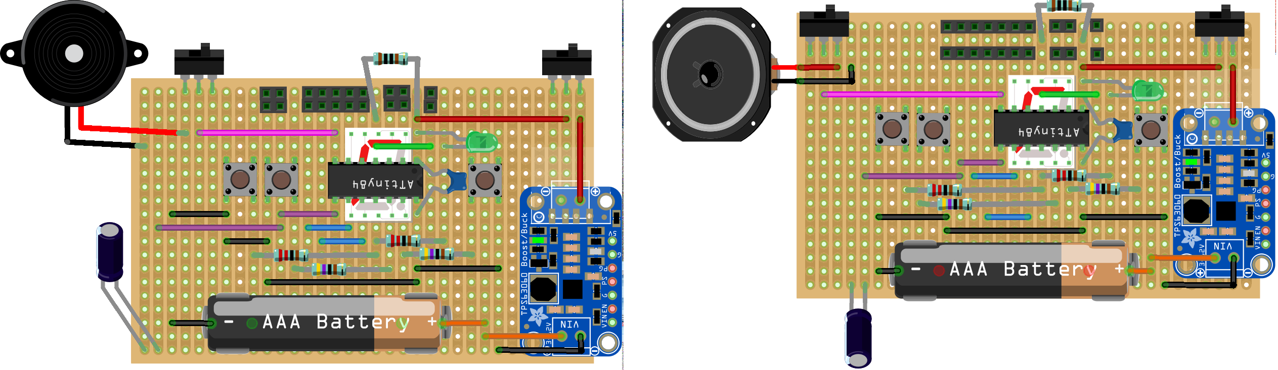
The new speaker placement has led to changing the layout on two main points:
- The speaker terminals now connects to different PCB traces. In the previous layout these were spaced out a few traces apart to allow for soldering a piezo speaker directly onto the PCB. In this layout the speaker terminals connects to two adjacent traces through a female pinheader, soldered to the bottom of the PCB. The leftmost trace cannot be too close to the edge of the PCB, or the pinheader will get squeezed between the PCB and the threshold of the inner case.
- The new battery holder has a smaller PCB footprint. This allows for moving all components and wires down one step on the vertical axis. This is done in order to space the two parallel patchbay pinheaders apart vertically. This should allow for easier user access.
Since I was changing the layout anyway, I took the opportunity to reorganize the patchbay pins slightly—the leftmost "gap" in the pinheader row is now eliminated.
Here's the PCB layout before and after:
I'm not convinced that the electrolytic capacitor is really doing anything useful at this point. I originally put it there to prevent DC current to flow across speaker terminals indefinitely. Since then I've tried to make sure the MCU will disable its speaker outputs at any time when sound isn't actually being produced. But I'm keeping it in there for the time being, mostly because I've seen other similar designs use a cap there, and I want to play it safe.
Discussions
Become a Hackaday.io Member
Create an account to leave a comment. Already have an account? Log In.