 Kevin Neubauer
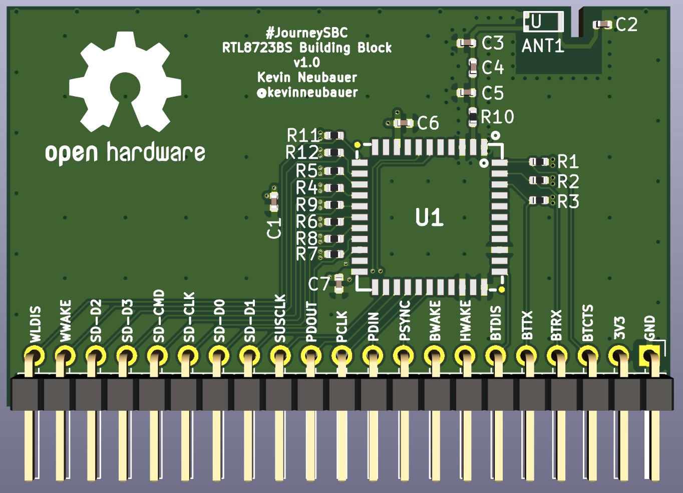
See here for the initial board stack up and features. Things haven't changed a lot between the initial draft and now. What has changed is via stitching/fencing, and the use of 2.54 mm header pins instead of the 1.00 mm header pins. I hate making a bigger board than I need for components, but it is what it is. 1.00 mm header pins aren't cheap or easy to find.
KiCad files posted to my GitHub. Link is on the main project page. If you like this design block and want to use it in any of your projects, you may want to wait until I get this assembled and tested.
Discussions
Become a Hackaday.io Member
Create an account to leave a comment. Already have an account? Log In.
Hi @mbt28. That is an interesting technique! What footprint do you use on the PCB?
Are you sure? yes | no
Hi,
You can use 2.00mm pin headers, I personally use 2.00mm like an edge connector too. Because it fits perfect to the most of the pcb sizes edge. If you are interested I can send you a picture too.
In addition to that I think you can put more grounds to connectors.
I added the 3 view: https://framapic.org/FCoABZfvtwuA/G7MTtAqUt8UJ.png
Are you sure? yes | no