 Kevin Neubauer
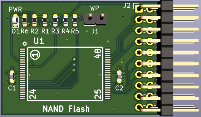
I thought I would have no way of building a standalone peripheral PCB for testing out the NAND flash chip I wanted to use. I had no CPU & RAM mainboard yet and no other interface chips to work with the raw flash. Then it hit me. At the Hackaday Supercon this year, I took an FPGA workshop that was led by @Piotr Esden-Tempski. It was called "WTFPGA?" and I would highly recommend it if you want an into into FPGA technology. I looked around for existing OSHW designs to use (because why reinvent the wheel?) and lucked out. A company called Waveshare produces a (mostly) OSHW FPGA NAND interface board. They publish the schematic and pictures of the board, but I could not find board layout files. However, I am confident that with the schema and pictures, I could reproduce what I need for my flash chip.
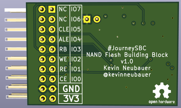
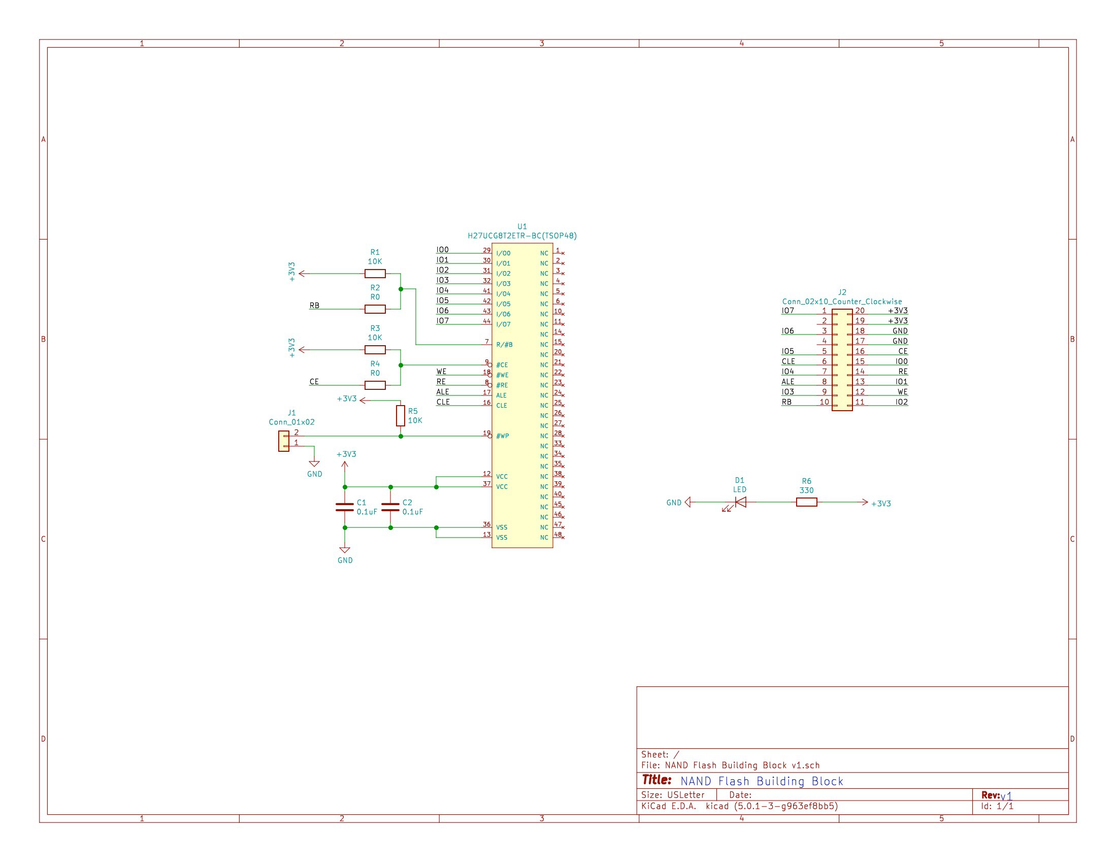
After drawing up my own schematic, I set to work on the board layout. This board should allow me to test out my NAND, and after I'm done with it, I will be left with an added bonus. I will have a NAND module to play with for my new FPGA setup.
Four layer board stack-up:
- Top: Signal traces and components. Remaining space filled with ground pour.
- Layer 2: Ground plane
- Layer 3: 3v3 Power plane
- Bottom: Signal traces. Remaining space filled with ground pour.
Components:
- SK Hynix H27UCG8T2ETR-BC TSSOP48 NAND (8 GB)
- 0603 Passives
Discussions
Become a Hackaday.io Member
Create an account to leave a comment. Already have an account? Log In.