 xBeau
xBeauFrom: Voja Antonic (via hackaday.io chat)
Board dimensions: 125×97.5 mm
Mechanical positions (X=0, Y=0 at bottom left):
Mounting hole: X=103 mm, Y=91.25 mm
Pin 1 of the expansion connector: X=4.90 mm, Y=81.35 mm
Pin 9 of the expansion connector: X=24.60 mm, Y=86.27 mm
Angle of all keys and expansion connector: 14°

 Arya
Arya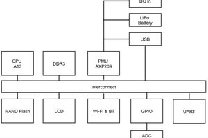
 Kevin Neubauer
 anfroholic
 Jon Thomasson
For a second there I was like: where did he get a white one? Ha!