 Dylan
Dylan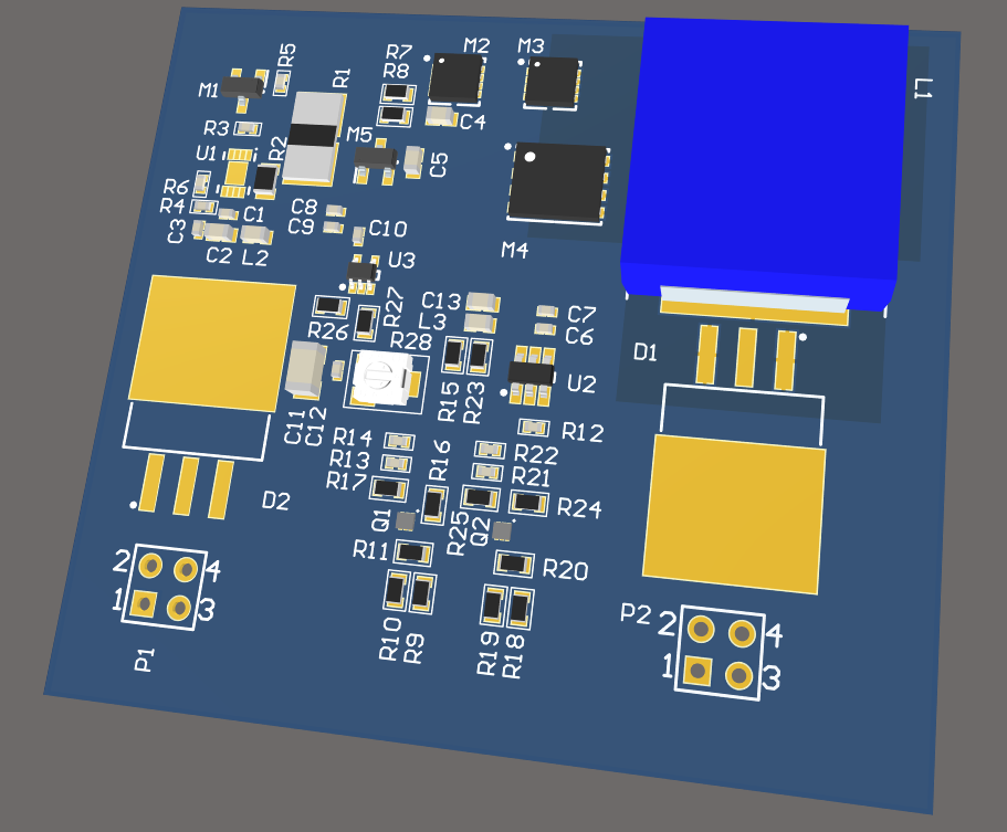
With the layout now complete, now routing and then off to the board house it goes. Of course if DRC doesn't give me a headache.
While being compact is certainly an end goal, testing will be a hell of a lot easier with a single sided board. Soon enough the 2 x 3.25 in board will be able to be shrunk. Probably put all the timing controls on the bottom, leave the big stuff on top for ease of manufacturing.
This board isn't anything fancy, just 2 layers, normal tolerances etc. Those dinky little double BJT packages (Q1, Q1) though are laughable given the comparison to that massive inductor in the top right corner (L1). Of course after looking at it, now I see that L1 is facing the wrong way. No big deal, but kind of annoying given everything else is fine.
The two connectors towards the bottom corners are the input and output connections. One for power in, the other for connecting to the supercapacitor. I thought it would be better to make it more universal without soldering the cap to the board, though for later revisions having presoldered caps would be nice.
All that's left to add in is some test points and maybe two or three mounting holes, because why not? Also can't help but add in some fun silkscreen stuff later on, but that'll be for later today.
Now on to routing!
Discussions
Become a Hackaday.io Member
Create an account to leave a comment. Already have an account? Log In.