 Stefkuhb
So I found the lines I soldered the wires and hooked up my logic analyser. lets see what is on those lines. I turn on the livingcolors, turn the LEDs on with the remote and start logging, no data. than I start logging and I use the remote to change the color, yes data!
This means that the controller is not polling the CC2500 for data but how does the controller know there is any data to read? The CC2500 is a slave and cant start to send data on its own, It must let the controller know it has any data. Probably there is an extra line to trigger the controller to read the data.
In the datasheet of the CC2500 it states that there are 3 configurable pins GDO0, GDO1 and GDO2 that can be used to give a signal to the controller. The function of these pins must be configured and this probebly happens when the system is powered. So I start logging and apply power to the LivingColors, again data but now its different. The datasheet of the CC2500 explains how to read and write a register.
All transactions on the SPI interface start with a header byte containing a R/W bit, a burst access bit (B), and a 6-bit address (A5 – A0).
The CSn pin must be kept low during transfers on the SPI bus. If CSn goes high during the transfer of a header byte or during read/write from/to a register, the transfer will be cancelled.

This means when the SS (CSn) line goes low the controller sends a header byte containing an address of the register, if it is a read or write command and a burst access bit.
The addresses for the function of GDO0, GDO1 and GDO2 are 0x00, 0x01 and 0x02. When I look at the data of my logic analyser it contains the data I'm looking for, 0x00 and 0x02, so GDO1 is not used.
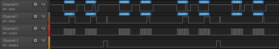
The controller writes 0x00 which is a header byte to write register 0x00 and then writes 0x06, the data for in the register. after that it writes 0x80 which means read register 0x00 and the MISO line shows 0x06 so its successfully written. 0x01 is written to register 0x02. The description of the value 0x06 for the GDOx_CFG of GDO0 is:
Asserts when sync word has been sent / received, and de-asserts at the end of the packet. In RX, the pin will de-assert when the optional address check fails or the RX FIFO overflows. In TX the pin will de-assert if the TX FIFO underflows.
The description of the value 0x01 for the GDOx_CFG of GDO2 is:
Associated to the RX FIFO: Asserts when RX FIFO is filled at or above the RX FIFO threshold or the end of packet is reached. De-asserts when the RX FIFO is empty.
I want to see if there is any signal on both GDO0 and GDO2, so I follow the signal lines on the PCB and see that both these signals have a testpad! GDO0 is connected to TP306 and GDO2 is connected to TP307. Next up: lets see when there is any signal present with my logic analyser.
Discussions
Become a Hackaday.io Member
Create an account to leave a comment. Already have an account? Log In.