 Keith
KeithOne of the first boards, it aimed to provide a full CP/M development system.
It was found that customers would develop programs on bigger machines, and wanted very simple Z80 boards for putting into control systems.
I'm not sure where I want to go with this. Floppy disks are pretty much dead, and the 64K DRAM and controller chip can be replaced by a simple 32K SRAM chip.
The SCPUB has the obsolete stuff thrown off already, and is easier to modify to run CP/M, because it has four JEDEC memory sockets.
I was recently contacted by someone who had this board with CP/M boot ROM and disks. I have reverse engineered the firmware into source code, which gives a good view of how it works. This should be useful for porting to my other STEbus Z80 board.
The PCB is four layer, because the DRAM chips take large current pulses. Modern SRAM chips are cheaply available with 32K, 128K and 512K so the design could be modified to use SRAM and a 2-layer board.
The first 32K of memory space could be ROM, RAM or up to six 32K pages (192K total) of STEbus memory. The design could be modified to use up 32 pages of STEbus, 32 pages of RAM and 32 pages of ROM.
My own board is salvaged, it was missing a PAL, boot ROM and disks. It may have other hardware faults that caused it to be written off by the test engineers. I have fitted copies of Steve's PALs and ROM and it now boots up to the stage where it asks for a system disk.
Steve's board is working to the same stage but has had problems setting the FDC timings and his drives are a bit rusty. The WD2791 FDC chip (£30 from ebay) is suspected.
The WD2793 is similar but with a true data bus ( £28 from ebay) so the latter could be used with minor mods to the firmware. These are used in the Atari machines, available from Best Electronics for $16.
 fjkraan
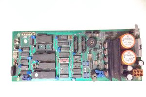
 Ken Yap