 Tony
Tony
Design
When it comes to design I trust the engineers from big semiconductors company. Why reinvent the wheel when it’s been done before; and by people that have a full time job in the field? So I took the 350V example from Linear, and adapted it to output the proper 170V Nixie voltage.
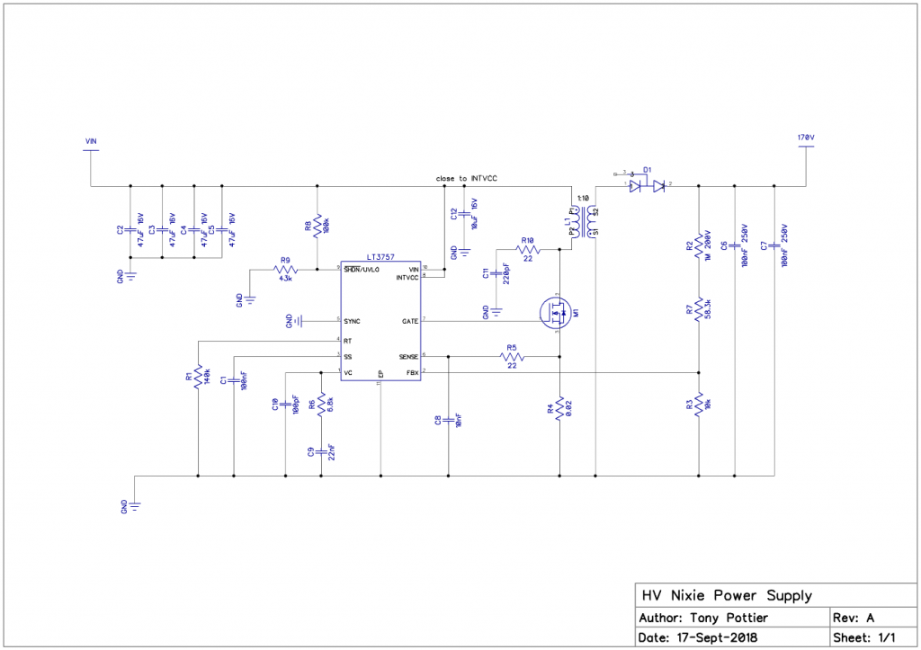
I even copied the weird double diode that they used; because I wanted first and foremost to have a working prototype before doing further changes. I just made sure the duty cycle would be OK with this new ratio and changed the feedback resistors but other than that: it is stock “typical application”.
Simulation
The good thing about working with Linear products is that they are incredibly easy to simulate since they provide all the models on LTSpice. So simulation is the next logical step in the design phase:
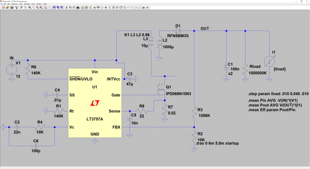
I have a love/hate relationship with LTSpice. On one end it’s a powerful tool; on the other end its user experience from Windows 3.1 era could not be more frustrating to work with.
That being said, it is interesting to use because you can predict the sizing and power dissipation of components pretty accurately. For instance that’s how I detected that the 22 Ohm snubber can’t be a typical 1/10W 0603 resistor. It was absolutely beneficial to be able to simulate the design

Another interesting piece of information picked up from the simulation is predicting the voltage spikes at the drain of the transistor.
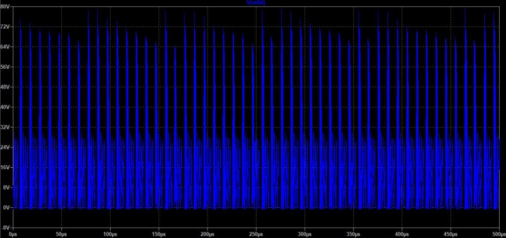
These spikes are cause by the inductance leakage in the transformer and will absolutely kill the MOSFET if it’s not properly avalanche rated. In LTSpice, this behavior can be simulated by using a less than 100% coupling coefficient. The DA2032 transformer specifies an inductance leakage of 0.150uH. That’s 0.150 / 10 = 0.015 or 1.5%. Rounded up to 2%, I used in the simulation a coupling coefficient of 1 – 0.02 = 0.98.
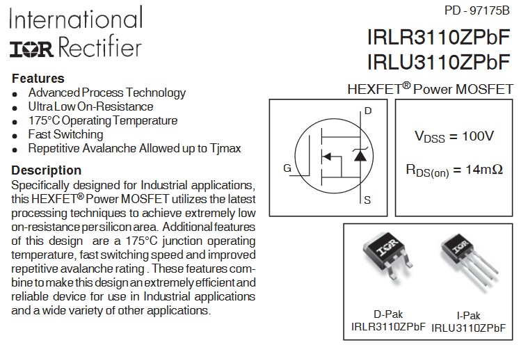
To be on the safe end, I decided in the end to go with a 100V rated MOSFET. Linear engineers went with 60V on their 350V application but I decided it doesn’t fit with the “build like a tank” design goal. Picking a MOSFET is not an easy task, there are thousands of reference out there. I used Mouser to quickly give an idea of what to look for:
- 100V rated
- SMD/SMT
- A friendly package (no bare dies and weird proprietary packages)
Even with these restrictions, you are still left with over 200 results!
So now comes the dance of finding the right balance of low resistance, low gate charge, availability and cost. It is a painful process, but one that needs to be done and a good exercise in navigating the semiconductor industry’s jungle. In the end I found the one in the name of IRLR3110ZPbF. At 12mOhms Rds(on) and 34nC total gate charge, it is an extremely efficient switching MOSFET. In addition, it is rated “active and preferred” by Infineon meaning at the time of doing this prototype this part has no risk of being made obsolete in the near future.
Discussions
Become a Hackaday.io Member
Create an account to leave a comment. Already have an account? Log In.