 Tony
Tony
PCB Prototyping
Thanks to lots Shenzhen-based companies, producing PCBs is cheaper than it has ever been. Coupled with extremely aggressive pricing on shipping and you can basically get yourself professionally made PCBs delivered to your doorstep in about a week for less than US$30. Isn’t it a beautiful thing? Some people are still sad you can’t simply prototype on a breadboard with all these pesky SMD components. I say it’s a trade-off I am more than willing to accept! So the next logical step was to design a PCB.
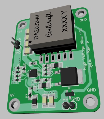
This is the first design (Rev. A) I came up with:
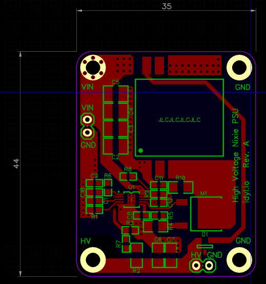
Looking back, I see now straight away issues: the input voltage going through vias, ground and high voltage pins being way too close to each others; and this high frequency signal coming out of the transformer being dragged all around the board to the diode. As they say hindsight is 20/20.
First results
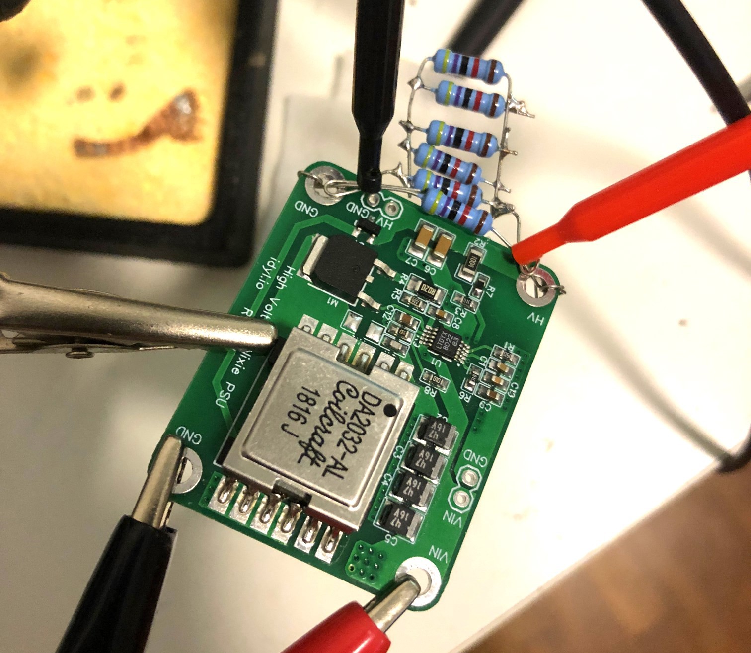
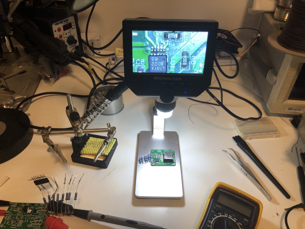
First of all it’s amazing to see this thing work for the first time. In order to work with 0603 components and the tiny 0.5mm pitch regulator you absolutely need a microscope. It’s almost impossible to see solder bridges with the naked eye.
The other key ingredient to make this work is a stencil. Nowadays the PCB fab will ship you a stencil together with the board for a few more dollars. It’s just not practical to use solder paste with a syringe when you have pads so small. Everything will bridge and you will spend a ton of time fixing the board. Stencils are 100% worth their money.
The thing is, even with a stencil some 0.5mm pads will bridge up, because it’s applied by hand over the PCB stencils holes the amount of paste left will never be as good or as precise as a machine perfectly aligned with it. As with everything: practice makes perfect.
Reading 170V on the multimeter at the output is really reassuring and a good sign!
However, I could only see an efficiency of about 75%. It’s not awful considering the boost ratio we are dealing with, but it’s still miles away from what LTSpice had predicted. I found two culprits:
- The Vishay double diode: it’s a wasted voltage drop party in here, I’m sure we can do better.
- The Snubber network: I purposedly chose a higher voltage MOSFET so I can also get rid of this waster power.
For the 2nd case, I simply unsoldered the 22 Ohm resistor part of the snubber network and efficiency immediately rose up to 80%+. For the diode, that will unfortunately need a revised prototype. It’s ok, I can improve the layout at the same time!
Discussions
Become a Hackaday.io Member
Create an account to leave a comment. Already have an account? Log In.