 Benchoff
For this build, I have extended these techniques slightly by mechanically bonding the layers of PCBs together with solder. This was previously done by Voja Antonic and his work in building enclosures out of FR4. His approach was to create a strip of bare copper around the perimeter of each side of the enclosure. By mounting these sides of the enclosure at the correct angle, soldering the two flat planes of PCBs into a three dimensional shape is as simple as running a soldering iron over the exposed copper on the perimeter.
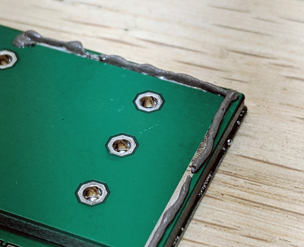
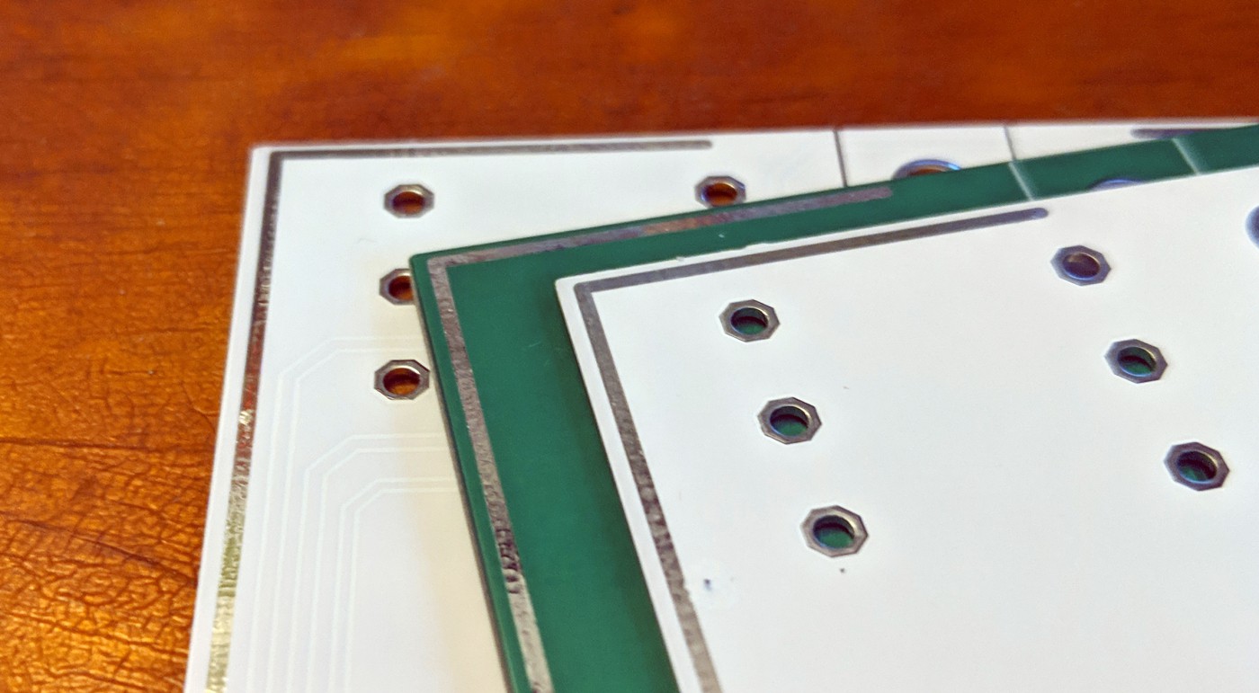
Each PCB in the stackup has exposed copper along the perimeter. By applying solder paste and clamping the boards together they’re read for reflow.
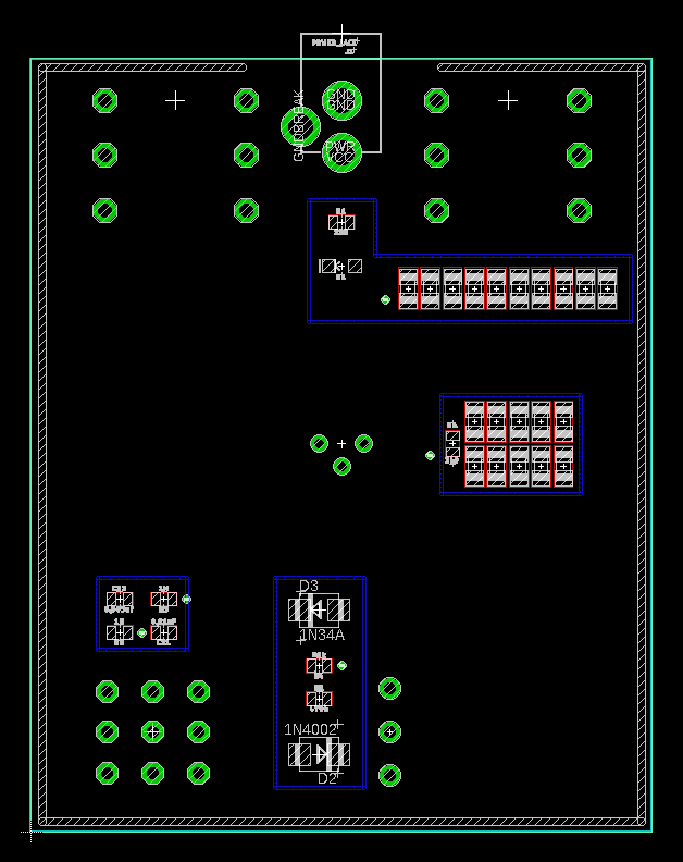
This circuit board was first constructed by laying out the through hole components in logical places, then dropping the surface mount components in places that made sense. Again, this is an exceedingly simple circuit with less than a dozen parts, in the schematic. Once that was done, it was only a matter of copying the PCB to a new file and adding cutouts around the parts. This board was done in Eagle, giving me the ability to add many layers to the board which could then be added to the CAM manager to create the Gerbers.
The real ‘trick’ with this technique is encapsulating components within a PCB stackup. While this can be done with a standard PCB thickness of 1.6mm per layer (three layers are required for complete encapsulation, resulting in a final thickness of 4.8mm), I used 0.6mm thick PCBs for the top and bottom layers. This resulted in a final thickness of 2.8mm. This is thin enough that the assembled piece does not register in your mind as a stack of PCBs. It’s thin enough that one could easily believe this is just a normal PCB.
It’s easy to create a PCB, and if you know what your board house can do, it’s easy to create internal cutouts on a board. There is absolutely nothing new about the previous thousand words. The trick to Oreo construction is mechanically bonding the layers together. This could be done with glues and resins, but taking a page from Voja’s work, I decided to use solder to attach one layer of PCB to another. This was done by a copper trace around the perimeter, disconnected from any ground planes or pours.
The assembly process is as simple as populating and soldering the bottom layer board with surface mount components, preferably with lead free solder paste. Then, leaded solder paste is applied to the perimeter traces, the boards are clamped together, and the entire assembly is thrown into the reflow oven. After that, it’s simply a matter of populating the through hole components.
There are other ideas I considered to connect these different PCBs together. I could ‘stitch’ them together with vias and through holes, using small bits of wire to both align and mechanically attach each layer together with solder.
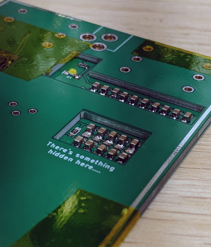
While you can embed capacitors, resistors, and microcontrollers inside a stack of PCB, there are limitations. First and foremost, the Rangemaster clone circuit calls for 47 μF capacitors. This value is much too large for small SMD caps, and the (physically) smallest caps I can find with this value are on the order of 10mm thick. Unless you want a circuit board that’s half an inch thick, these caps are far too large. The workaround for this problem is to add many caps in parallel.
This leads to another problem. The original circuit used electrolytic capacitors, not small ceramic capacitors. Because I’m using arrays of ceramic caps, the actual capacitance is less than the sum of all the capacitance in the array. MLCC capacitors should be derated when biased (as they are when using them as a bypass cap), and the capacitor I ‘constructed’ does not have the correct value in the circuit. Yes, the capacitance of ceramic capacitors is dependent on their voltage, but you can aaay yolo around this by simply adding even more capacitors.
small boost power supply, you probably have a relatively large inductor. Inductors of a sufficient rating for a beefy power supply will be too tall to embed into a single layer of FR4. The same is true for components handling high power, as they’re usually physically large and must dissipate heat, the latter being a problem for a component that is effectively trapped inside a fiberglass box.
Despite the problems, this is an interesting technique of PCB fabrication. Combined with the dropping prices of custom-made PCBs — the boards for this entire project cost less than $15 USD total — I would expect to see many PCB artisans picking up this technique.
This project was just a demonstration of what is possible with Oreo construction, but given the huge advancements in artistic PCBs, this is in no way the limit of what is possible. Given we’re now in the golden age of reverse-mount LEDs, it’s possible to encapsulate the driver and the LEDs of a gigantic matrix inside fiberglass. With Oreo construction, an entire PCB could be just a brick of fiberglass when it’s off, and a glowing rectangle when it’s on.
Discussions
Become a Hackaday.io Member
Create an account to leave a comment. Already have an account? Log In.