 Foxchild
- Part 1: How the sound is made
- Part 2: How the CPU does what
- Part 3: Writing the first ROM file
So, as promised, we're going to write our first SNES program today. There are many tutorials out there for SNES code in assembler language, but we're going to do things a little differently today: We're going to write bare-metal machine code right away!
Tools needed:
- HxD: A Hex editor for Windows
- bsnes+: A SNES emulator with debugging tools
We'll have to use bsnes+ because it's emulating hardware and it's not focused on playing SNES games. Emulators like 9snesx will not work because they ommit certain hardware "features" (and bugs). The bsnes+ emulator simply takes machine code from a binary file and feeds it to a virtual 65816 processor in a SNES machine. bsnes+ also emulates SPC-700 and other chips in the SNES. To write our first program we have to understand at least a little bit about memory mapping in the SNES. Unlike processors of today, the Ricoh 5A22 (65816 core) does not have built-in memory. It has a 24-bit address bus and an 8-bit data bus, and everything is connected to these busses. Even the internal system registers. So, the ROM, the RAM, the GPU... everything is connected to the address bus and seperated into address spaces called a "memory map". To talk to the ROM, we have to use the correct address space.
As you can see in the Memory Map of the SNES (https://wiki.superfamicom.org/memory-mapping), ROM is located at Banks 0x00-0x3F on addresses from 0x8000 until 0xFFFF. So the ROM is located on 64 banks of 32768 bytes each. 64 times 32768 equals 2097152, which equals to 2MB. There are ways to address much more space on the SNES, but for now, we don't care about this.
A bit about the ROM model on the SNES:
There are two typical types of ROM for the SNES called LoROM and HiROM. I will only focus on LoROM. LoROM causes ROM chunks in SNES to be max 32KB wide ($8000 bytes), and are typically fetched from the $8000-FFFF region. It is produced by connecting the address lines like this:
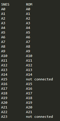
So for addresses from 0x000000 up to 0x007FFF everything works "normal". Since A15 is not connected, the adresses from 0x008000 up to 0x00FFFF refer to the same area. Same with the banks. Since A23 is ommited, the ROM can only distinguish between adresses in the banks from 0x00 up to 0x7F (128 banks) and the banks from 0x80 to 0xFF refer to the same area. So the ROM is repeated once in every bank and the upper banks repeat too. But if we take SNES signals A16 to A23 (the bank lines), we can see that A16 is actually connected to A15 on the ROM. So the SNES counts the addresses from 0x000000 up to 0x007FFF, everything is cool, then it counts from 0x008000 up to 0x00FFFF and actually sees the same data. This means the ROM is now at address 0x007FFF.
SNES                 ROM

0x00:0000 -
0x00:7FFF           0x000000 -
                    0x007FFF
0x008000 -
0x00FFFF
Now the first bank bit increments and the SNES is at address 0x010000. The ROM actually sees this as bit 15 and reads the following address:
0x000000010000000000000000b: SNES 0x010000h
0x000000001000000000000000b: ROM  0x008000h
SNES                 ROM

0x01:0000 -
0x01:7FFF           0x008000 -
                    0x00FFFF
0x01:8000 -
0x01:FFFF
So, since one bit (A15) was left out, the ROM gets mapped twice on the SNES and has its own address space. This concept works for banks up to 0x1F, then things get a bit more complicated, but I wouldn't worry about it too much right now. One more important thing is that ROM is only visible from SNES addresses 0x008000 to 0x00FFFF, because the lower half is used for other things.
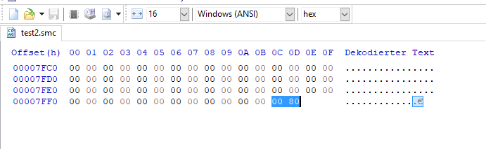
O.K., now back to our ROM file. The file needs a block of specific information which includes the internal name of the ROM, the interrupt vectors (addresses to machine code within the ROM in 16 bit format), version, etc. This portion of the ROM is also known as the SNES header. While the name of the ROM and certain region locks are not important, because they are only tested by software itself, it is very important to provide parts of the interrupt vector table. Then the 5A22 boots up, it starts looking for the first address to read instructions from. This address is called the reset vector. The reset vector tells the processor where it can find the first value for the program pointer. The are several other interrupt vectors and they all have a certain location in memory, but at this point we only need the reset vector. The interrupt vector table is located at the end of the first ROM bank, so around address 0x007FFF. The reset vector is stored at address 0x007FFC and 0x007FFD, but remember, this address corresponds to 0x00FFFC and 0x00FFFD for the SNES! In our ROM file, we look for address 0x007FFC and 0x007FFD and write the values for the first address of instructions IN SNES ADDRESS SPACE. So, instead of writing 0x0000, we have to write 0x8000, the the processor will start reading instructions from the beginning of our file. If, for some reason, we want to start writing instructions at address 0x000004 in our file, the reset vector has to have to value 0x8004. This is what the reset vector looks like in the ROM file:
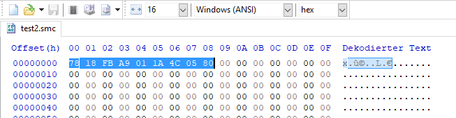
And now we write a very short counter for the 5A22. In the 65816 reference (https://wiki.superfamicom.org/65816-reference) we can find the instructions for the 5A22 and its hex values. We start by disabling interrupts with the SEI instruction. It has the hex value 78 and takes no operand. So, first address in our ROM file takes the value 0x78, that's it. Next address is 0x000001. For good practice, we start by setting the 65816 into native mode (because it always boots in emulation mode). This is done by issuing the instructions CLC (clear carry flag) and XCE (Exchange Carry and Emulation Flags) in sequence. Addresses 0x01 and 0x02 take the values 0x18 and 0xFB. Now we can write a little counter. First we have to load some constant value into the accumulator. We can do this with the instruction LDA (Load Accumulator from Memory) and providing an 8-bit constant. This means, addresses 0x03 and 0x04 take the values 0xA9 (LDA) and 0x01 (decimal 1). Next instruction is to increment the accumulator with the instruction INC A (Increment). Address 0x05 takes the value 0x1A. Since we want to repeat this incrementation, we have to jump back now. We can do this with the JMP (jump) instruction and providing an address in memory for where to jump to. Addresses 0x06 takes the jump instruction with the valule 0x4C and the addresses 0x07 and 0x08 receive the address to jump to, which will be the INC instruction at address 0x8005. That's it! Our program memory should look like this now:
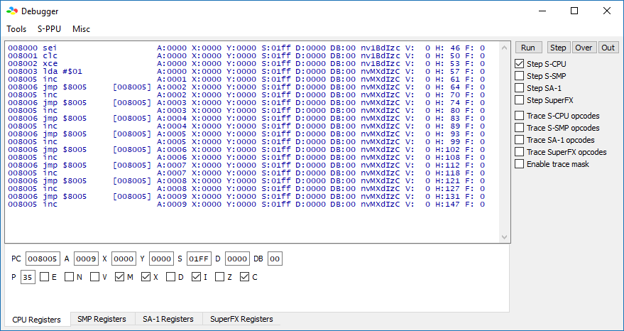
We save this file and try it with our emulator now. Open bsnes+ and go to Tools and open the debugger. Click on the break button so we can step through the execution of our file. Now load up the hex file that we've just created. Nothing happens, until we click on the step button once. As you can see in the debugger view, the instruction SEI was executed, so the reset vector was loaded and the SNES has started to execute instructions at this address! Awesome! If you press step three more times you can see the "E" checkmark in the bottom left corner disappear. This means that our processor has left emulation mode and is now in native mode! Sweet! If you click step repeatedly now, you can watch the accumulator increment its value. The jump instruction always resets the program counter to 0x8005. This is actually code that we can burn onto a ROM chip and execute with a real SNES, even though it wouldn't be very interesting to watch haha.
In the upcoming posts I will finally show you the hardware I created to simulate a real ROM chip with a STM32 chip and show you some measurements I did with a logic analyzer on all cartridge signals. There's a lot of content coming up!
Thanks for reading!
Cheers,
Michael
Discussions
Become a Hackaday.io Member
Create an account to leave a comment. Already have an account? Log In.