 Bud Bennett
This is a distillation of the thought process involved with putting this UPS together. There are always compromises to be made. I will go through the trade-offs involved with this design -- section by section. It's a bit long-winded, but I found it is best to put it into words before you spend money on parts/services. There was a saying in my engineering design circles, "If you can't explain how it works, you don't know."
Basic LTC4040 application
I haven't deviated much from what Analog Devices recommends for the LTC4040. Refer to the LTC4040 data sheet for particulars. I have included a couple of band-aids to help alleviate potential problems base upon my experience with the LTC4041 -- a supercap back up manager.
There are multiple ceramic capacitors at the load and also at the battery. This is normal SMPS procedure to place a smaller ceramic capacitor along with a larger ceramic capacitor at the input/output of the switching regulator. The smaller cap has a higher resonance frequency and tends to quell the HF stuff. The larger cap provides a lower Z but has a lower resonance frequency. The combination of the two capacitors covers a larger range and tends to prevent problems with ringing in response to switch transients. There is also a large tantalum capacitor, C4, which is a tank capacitor to hold up the output when the input power fails.
The input switch
The LTC4040 data sheet block diagram shows two input switches required to disconnect the input from the load. The basic application of the LTC4040 shows an NMOS FET connected with its source at the input and the drain connected to the load. This doesn't work for this application because the body diode of the FET will keep power applied to the load even if its gate is grounded. This application can get away with a single FET switch to disconnect the input from the load because the input source nearly always (always) becomes a high impedance when the AC power fails. In this case, M1 holds the input voltage at a diode drop below the output voltage because the FET drain-source is reversed. When IGATE is pulled to GND the FET turns off and allows the load voltage to drop to zero.
Note: if the input power source fails by shorting its output to GND then this approach would not work. In my experience all 5V AC adapters become high Z when the AC power fails.
The TSM038 is a logic level FET switch with 4mΩ Rdson, 30V BVDSS and can handle ± 20V from gate to source, which is necessary because the IGATE voltage can exceed 8V from gate to source. It costs about $0.60 in low quantities.
Safety First
I had originally intended that the battery charger parameters be programmed by a 3 position dip-switch. I got rid of the dip-switch when I upgraded the PIC controller to 14 pins, thinking that all the charger parameters could be programmed by the Raspberry Pi via the I2C interface. But this idea quickly fell by the wayside simply because it would expose the charger parameters to being hacked, which is a safety issue. So the dip-switches came back (albeit in SMD form) and the PIC is simply informing the Raspberry Pi about the switch settings and has no control over them. The user must set the dip switch positions when he/she installs the battery into the UPS.
I also implemented the thermistor sensor to prevent charging outside a safe temperature range. The sensor must be attached to the battery, not to the PCB, in order to be effective. I figure you can just tape it to the battery. Having the thermistor attached to the battery will prevent dangerous situations that could cause the battery to overheat and catch fire. At cold temperatures the battery electrolyte freezes so it is not a good idea to charge it under those conditions. The thermistor is a typical 10k NTC type with a B25/50 = 3950, which matches the desired temperature characteristic called out in the LTC4040 data sheet.
Additionally, the CHRG_ and FAULT_ status from the LTC4040 are monitored by the PIC and provided over the I2C interface. The Raspberry Pi might be able to communicate with the user if a fault condition is detected.
The PIC
With all of the added monitoring to perform, the PIC needed more pins. I knew that Microchip offered the PIC16F18323, a pin-count upgrade to the PIC16F313 that I had used previously, in a TSSOP-14 package that is approximately the same area as the SOIC-8 package used by the 8-pin version.
The PIC gets its power from the battery when the LTC4040 is shut down. When AC power is available the PIC gets power from the UPS output (~5VDC). A dual Schottky diode, D1, routes the highest voltage to the PIC power pin. When operating from the battery the PIC only draws a couple µA because it is in sleep mode. When active, the PIC can draw several hundred µA so it's best to get it off the battery -- to maximize the time between charging cycles and increase battery longevity.
In an effort to reduce component count the PIC uses its weak pull-ups instead of adding discrete resistors. The downside is that those weak pull-ups aren't so weak -- 200µA. When the UPS is powered up the weak pull-ups are engaged on FAULT_, CHRG_, F0-F2. When the LCT4040 is shutdown, and the PIC is running off the battery, weak pull-ups are disabled and those pins are driven to GND by logic outputs to keep indeterminate currents from flowing in the PIC input circuits when pins float.
AC presence detection, ACPR, is performed by the PIC when the LTC4040 is shut down, and by the LTC4040 when it is active. The PIC uses a resistor divider feeding a Schmitt Trigger input to get a rough idea of when power is available at the UPS input. The Schmitt Trigger is good for rejecting noise, and works well when the PIC is powered by the battery, but it is problematic when the PIC is operating from 5V. So whenever the PIC is getting power from the UPS output the ACPR input type is TTL, which has a VIHmin = 2.0V. If the LTC4040 PFI comparator detects that the AC adapter voltage has dropped below its threshold it pulls ACPR to GND and so informs the PIC that the power had failed. R22 reduces the current draw on the open-drain PFI_ output.
The PIC is now using an external pin, RC2, to monitor the battery voltage with an 8-bit ADC. I't pretty straightforward and there is a low frequency RC low-pass filter to reduce noise. The PIC has a 10-bit ADC, but it is a pain to implement the last two bits when all you have is an 8-bit µP. The resolution of the battery voltage is 16mV, which should be good enough.
R15 and R13 are probably not really required, but better safe than sorry. R13 just keeps the PIC from being reset until the pushbutton, S1, is pressed. There is an internal pull-up on the MCLR_ pin, but I don't know if it is always present. R15 is pure paranoia. As the PIC is booting up it floats all of its pins until they are assigned. It's better to have BSTOFF and CHGOFF set to VDD [2019-01-31 Edit. It was previously set to GND.] than float.
[2019-01-31 Edit: The first pass parts had problems because R15 was connected to GND rather than the VDD of the PIC. When the battery was inserted the PIC required some time to set the PWROFF pin high. This allowed the LTC4040 to apply backup power and force the output to 4.8V. Since this is identical to a failed power condition, the PIC just went with it and allowed the LTC4040 to continue its backup mission. If the RESET button was pushed it acually forced the LTC4040 into backup mode because the PIC reset condition allowed PWROFF to be low. If R15 is connected to BAT then the PWROFF pin is taken high and the LTC4040 is inhibited from applying backup power when the RESET button is pushed. After the RESET button is released the PIC continues to keep it high until it senses AC power is available. That is the correct functioning.]
The PCB Layout:
I've learned a few things about SMPS (Switched Mode Power Supply) design from the last few projects. There are a few things that you have to get right...the rest is small stuff. The things that you have to get right is the grounding and the switching nodes. Here's a view of the current layout around the inductor and the LTC4040:
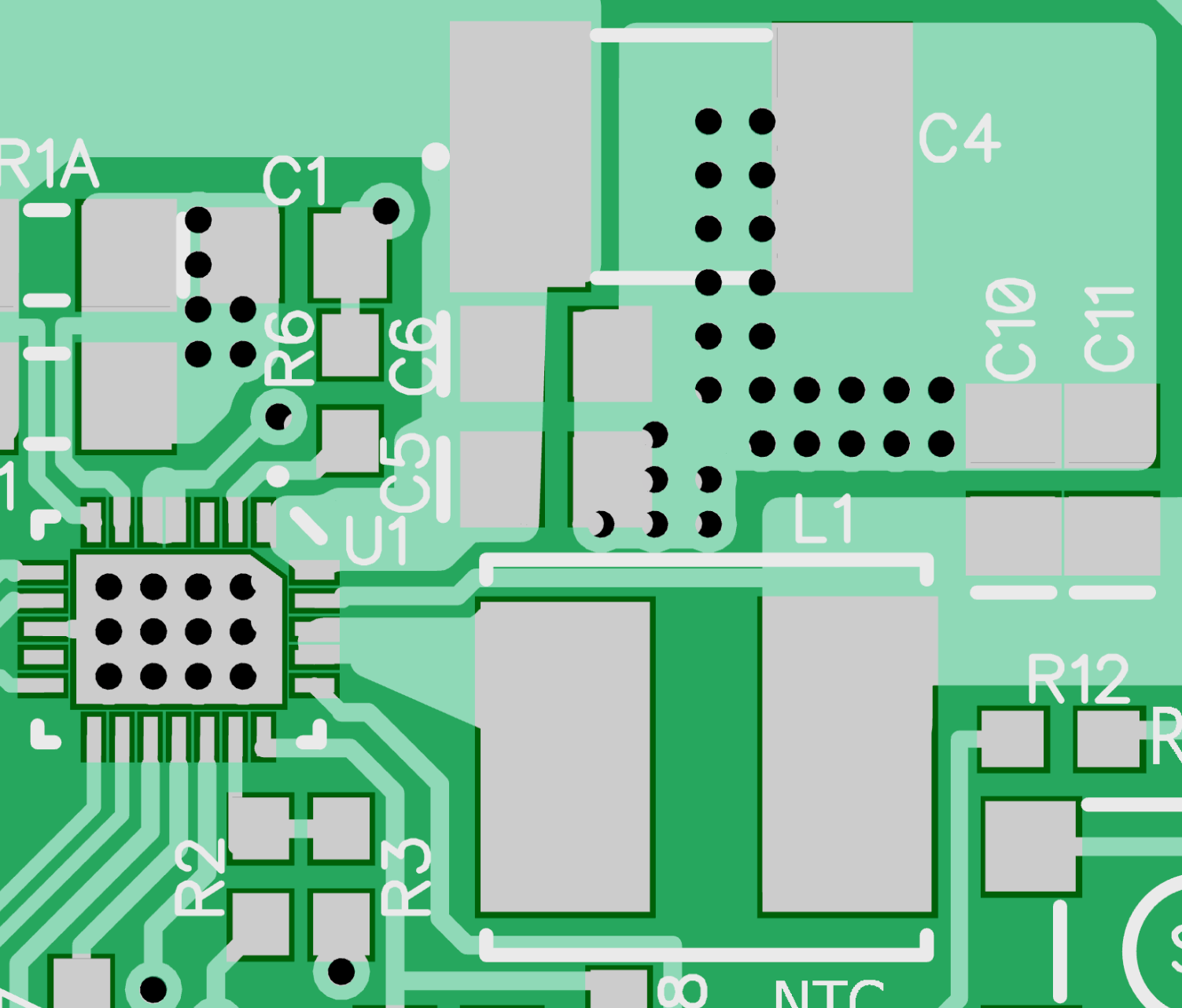
Note that the trace from the SW pins to the inductor is as short as possible. This node is switching 5V p-p at 1.2MHz with up to 8A! Note also that the distance from C5 and C6 to the VSYS pins is very short and wide -- keeping the parasitic inductance/resistance to a minimum. The exposed pad of the LTC4040 is completely covered with vias to the ground plane on the bottom of the PCB -- same for the GND returns for C5, C6 and C10, C11. This will keep the ringing to a minimum. The rest of the layout almost doesn't matter if you get this part right.
The pads on L1 are really large and quite close together. I've found that if you make oversized pads like this it allows for many sizes of inductors to be soldered to the PCB. I believe that almost any 7mm x 7mm or 6mm x 6mm inductor size will fit these pads, but it will need to have a saturation current and thermal rating of at least 8A.
Kelvin Connections:
It's important to use Kelvin connections when monitoring current flow through a resistor.
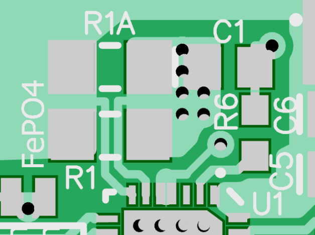 The pick-off points to sense the voltage across R1 and R1A are Kelvin. The current flow through those resistors enters from the left and leaves to the right. The connections to the LTC4041 that measure the voltage across R1 come from the inside of the resistor pads -- where there is the least amount of current flowing. This is done to avoid any spurious voltage drop caused by current flowing through the traces on the PCB and usually yields the most accurate measurement.
Other Layout Stuff:
Resistor dividers that are used to set comparator trip voltages or output boost voltage or SCAP charge voltage must be accurate. Therefore they are located fairly close to the LTC4040. Components that are not critical are move farther away.
Discussions
Become a Hackaday.io Member
Create an account to leave a comment. Already have an account? Log In.