 2-Zons
I was doing research for a new hobby project. I wanted to build a 68000 system on a bread board with I/O and possible video. As I dug deeper I started shifting towards maybe starting with an 8 bit CPU (6809) and then do the 68000 after. I'm pretty rusty at hardware, haven't done anything serious since the early 90's.
While doing this research I discovered a brilliant You-tuber named Ben Eater https://www.youtube.com/channel/UCS0N5baNlQWJCUrhCEo8WlA . He is an excellent presenter and educator. I watched his series on building an 8 bit bread board computer. He goes through step by step building a functioning 8 bit computer out of TTL logic. I'm sure many of you might be familiar with his work.
I've never really had a good understanding of the internals of a CPU. I knew that it involved state machines and registers but didn't really grasp how it functioned. In his series he broke down the computer into easy to understand blocks. After watching his series I was inspired to try and build something of my own.
Instead of building a simple computer, I want to build a self contained CPU that could be connected to a complete system (RAM, ROM, and I/O). I will use RAM and some I/O to build it but design it so it can be separated. I want to have some more advanced features on my CPU while trying to avoid feature creep. I do want to actually finish.
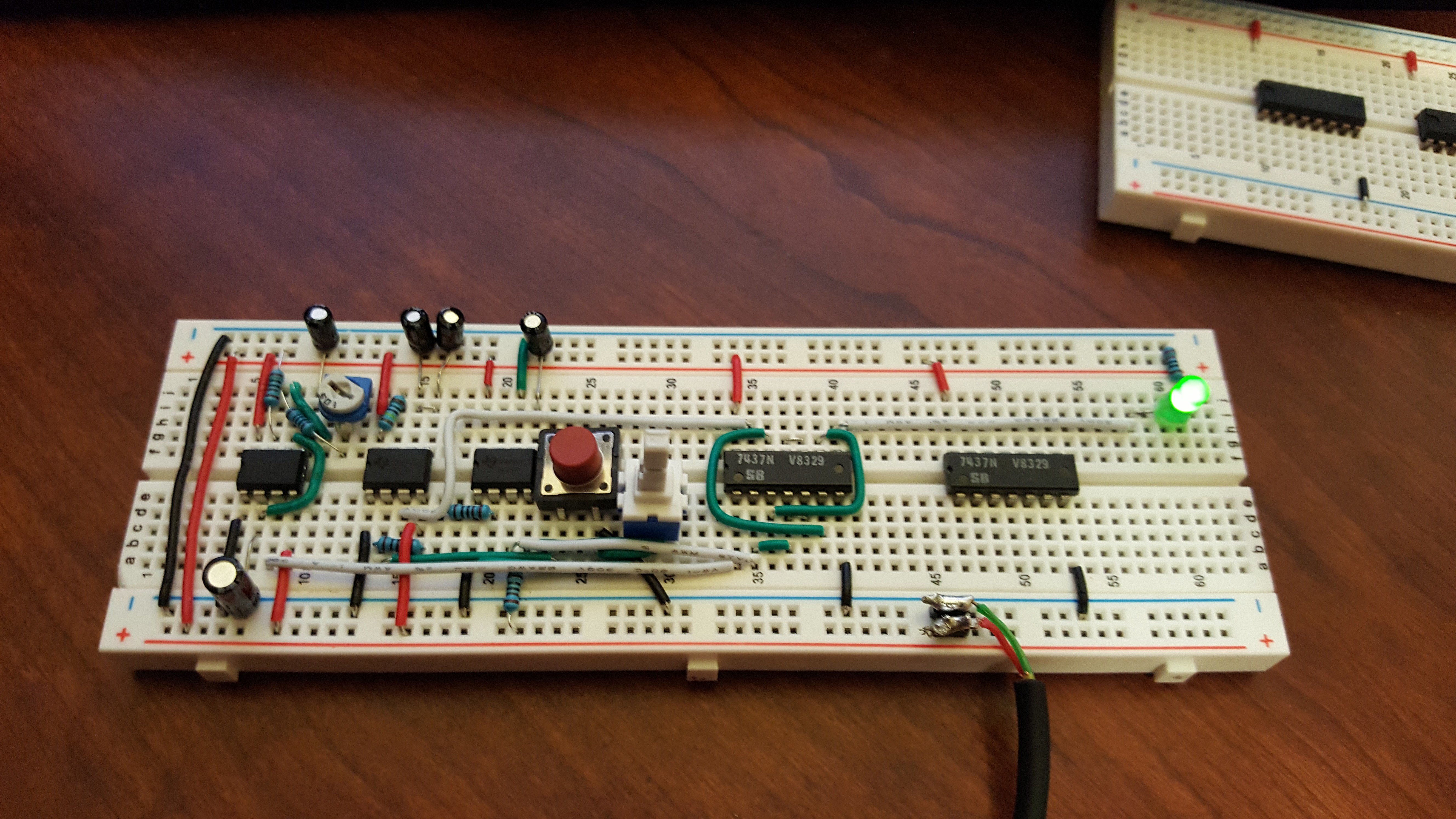
I've ordered a bunch of Breadboards TTL chips, resistors, LED's, DIP Switches, EEPROM's, RAM chips, hookup wire (8 colours), capacitors, 555 timers, toggle switches, and some other bits. I found a good deal on the long (63 row) breadboards on amazon. 3 boards for $12CDN with free shipping. I just received 9 of them today and they are superb quality.
I can't wait to get the rest of the supplies so I can start tinkering.
I've drawn up a block diagram for the basic design.
https://docs.google.com/drawings/d/1BW84zwO5effvYcdKjxzyki9cuvuHsM98z6nAamw4iTM/edit?usp=sharing
I've also started an instruction list which also has a page that lists the full names for all the control lines shown in the block diagram. Like I said I'm pretty rusty and not up to speed on normal naming conventions.
https://docs.google.com/spreadsheets/d/1kbxYGDeIOszgvjPYRdes-bELOBlojT_tjxe_RD9MVUQ/edit?usp=sharing
I've started an upverter project where I will be posting all the schematics.
Idea's and advice are most welcome.
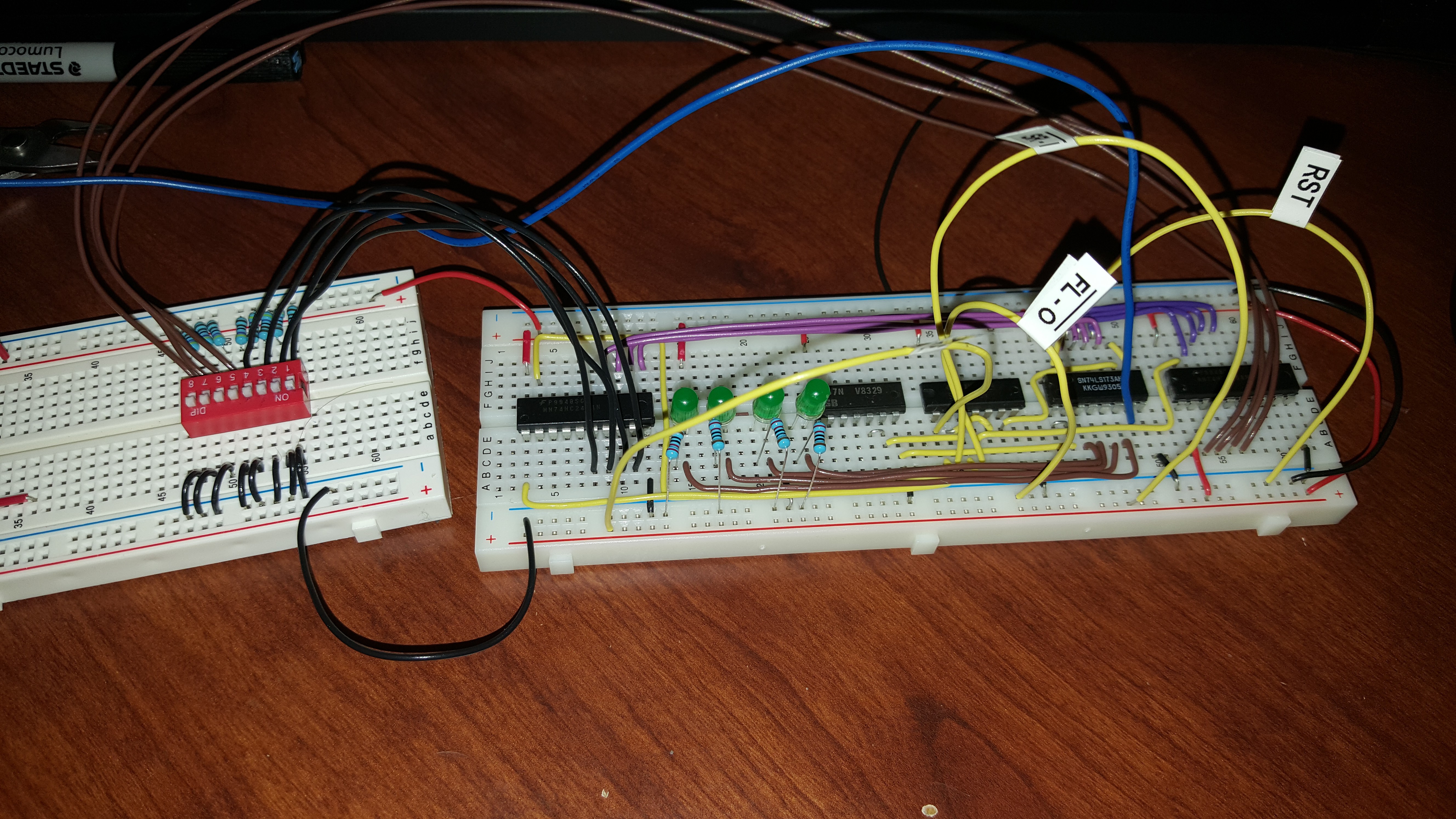
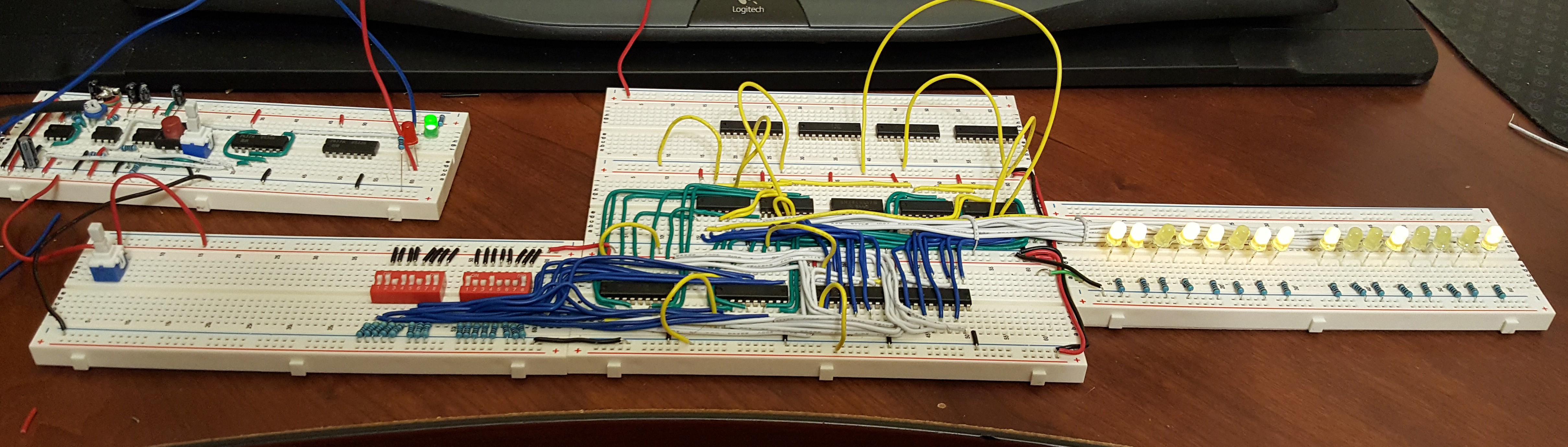
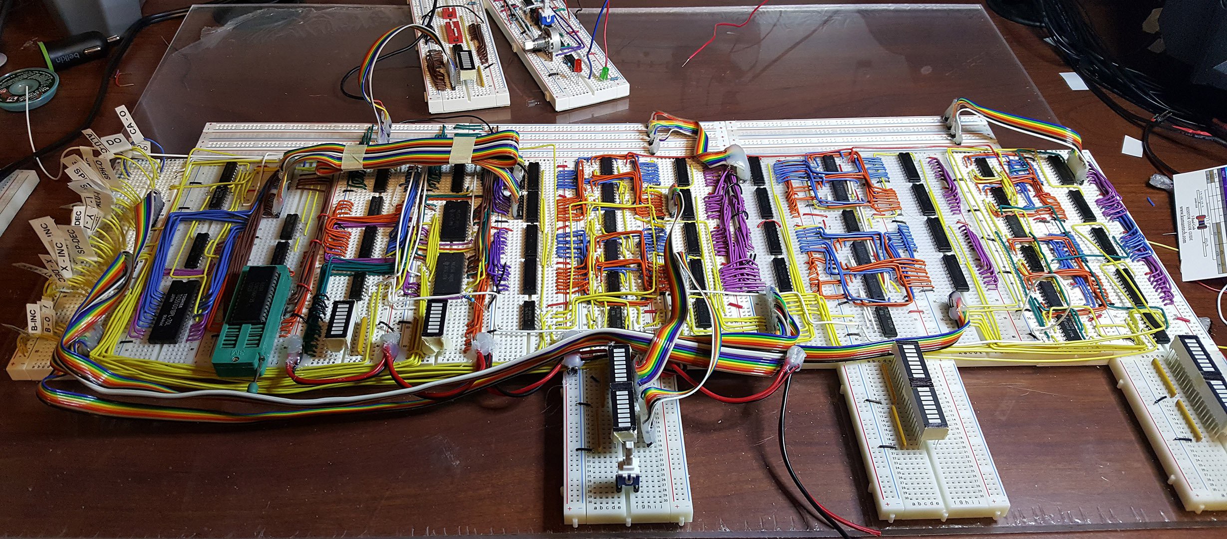 Finished routing all the control signals to a single board. Need to build a few more ribbon cables for the address bus, data bus connections and LED's. Looks much neater now. Modules completed thus far (from left to right in picture): RAM / ROM module, ALU, XY register, stack pointer, and AB register.
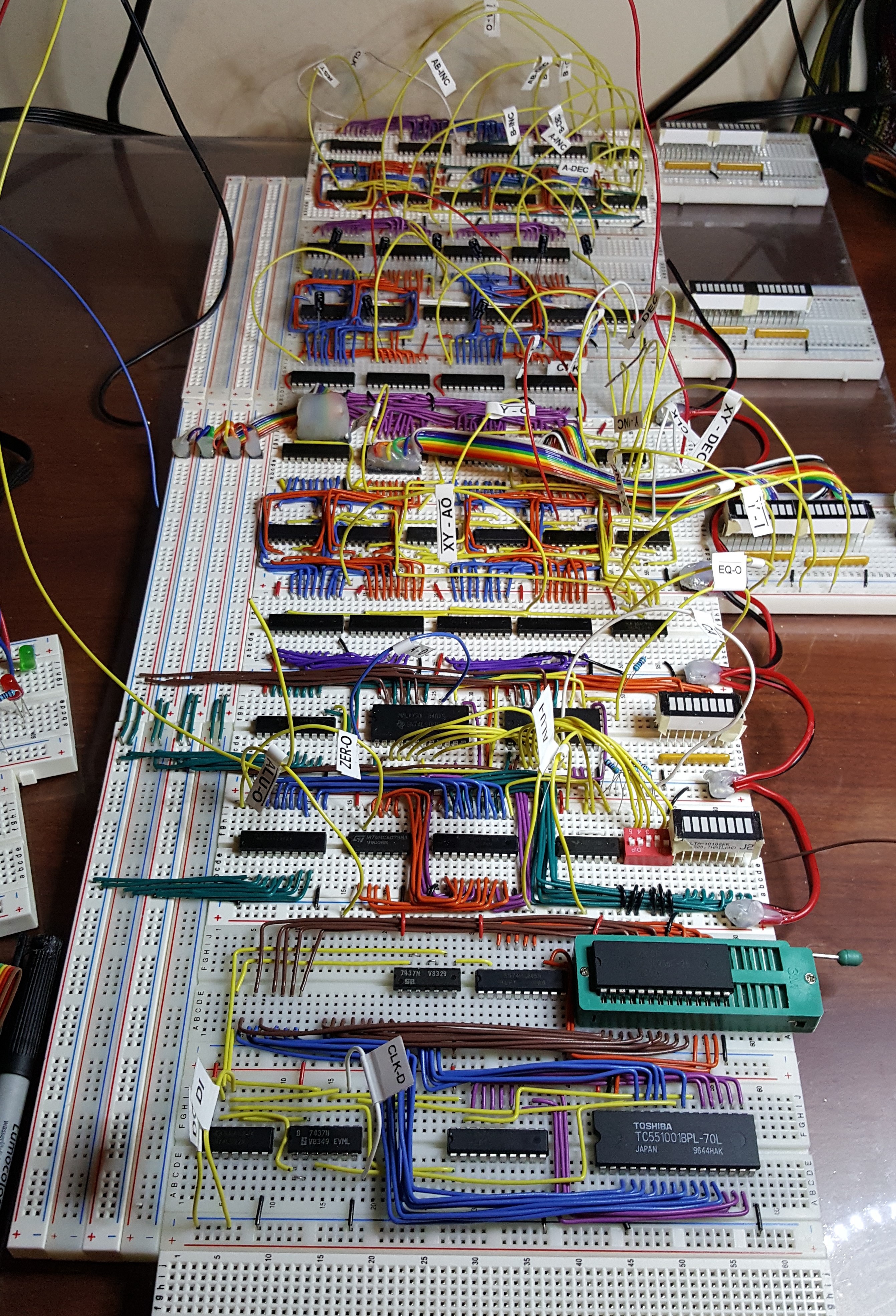
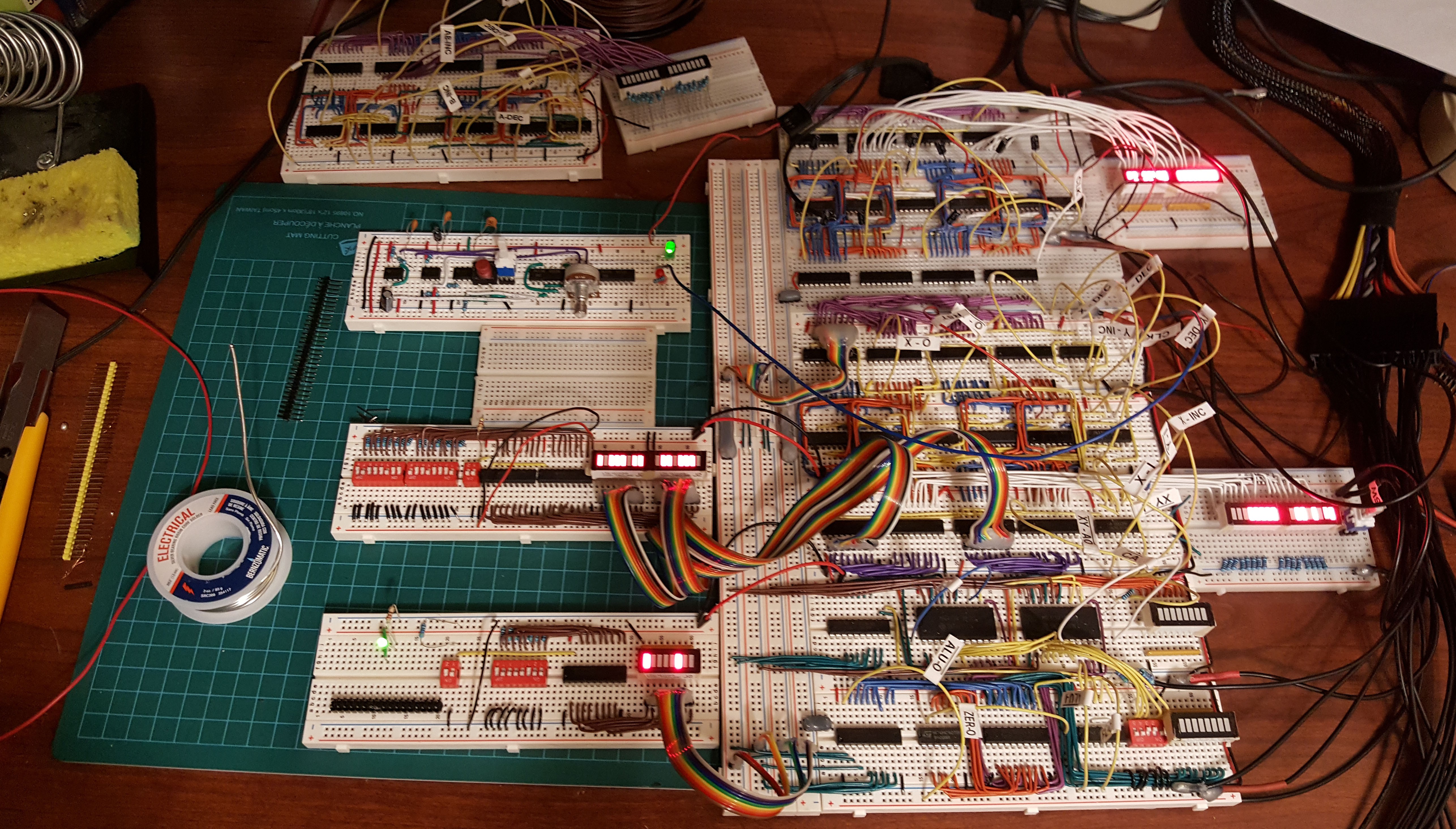
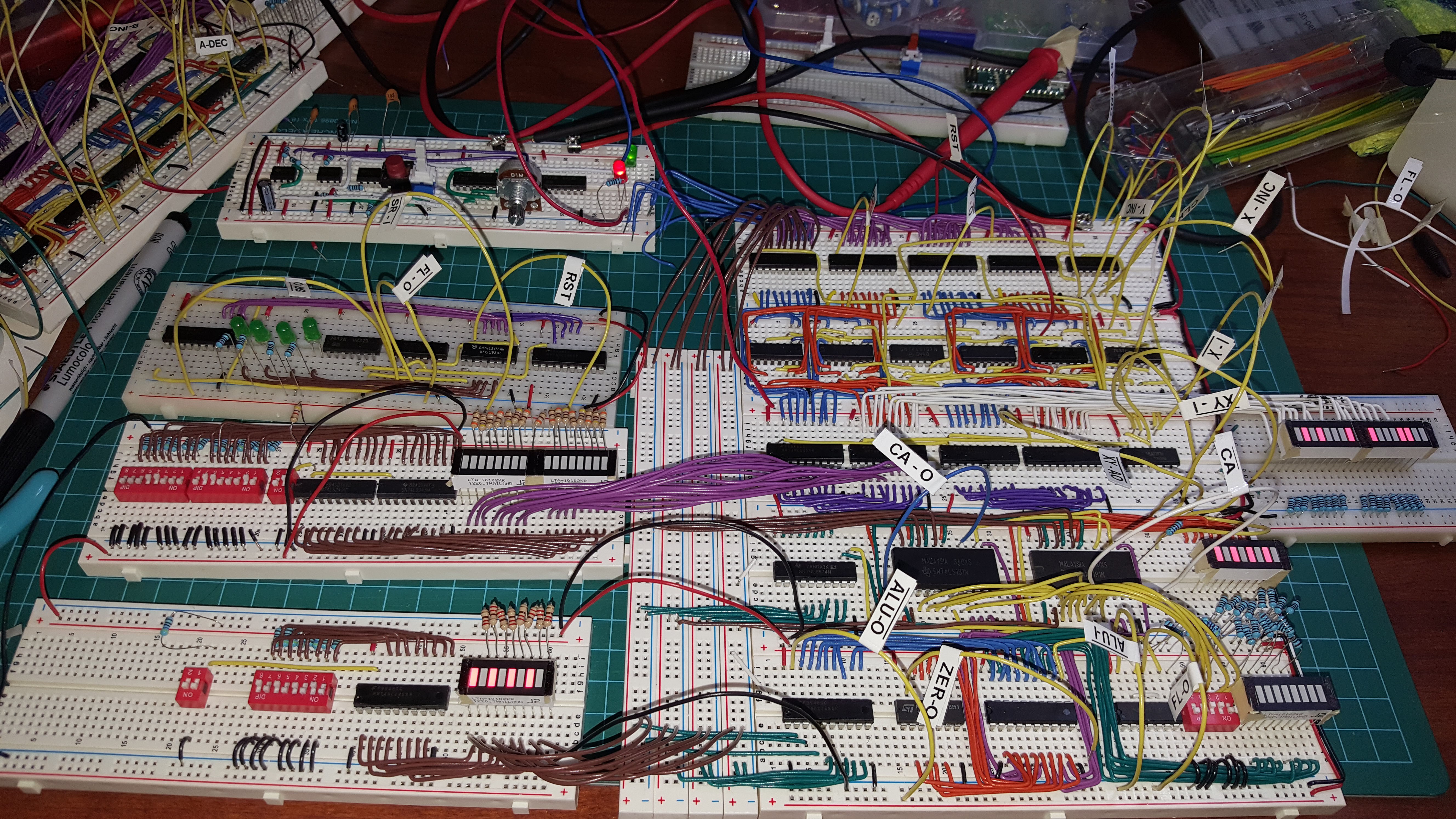
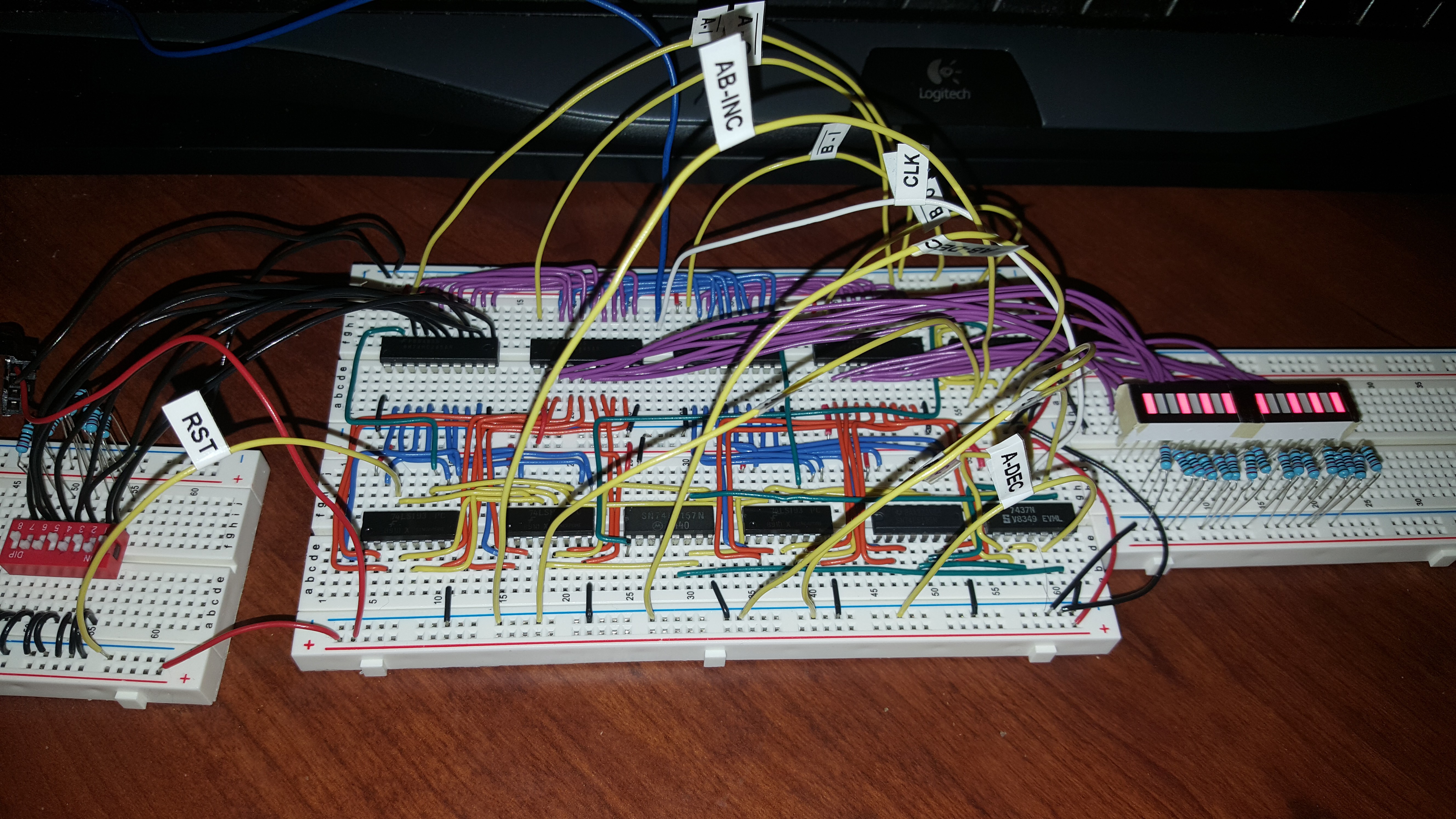
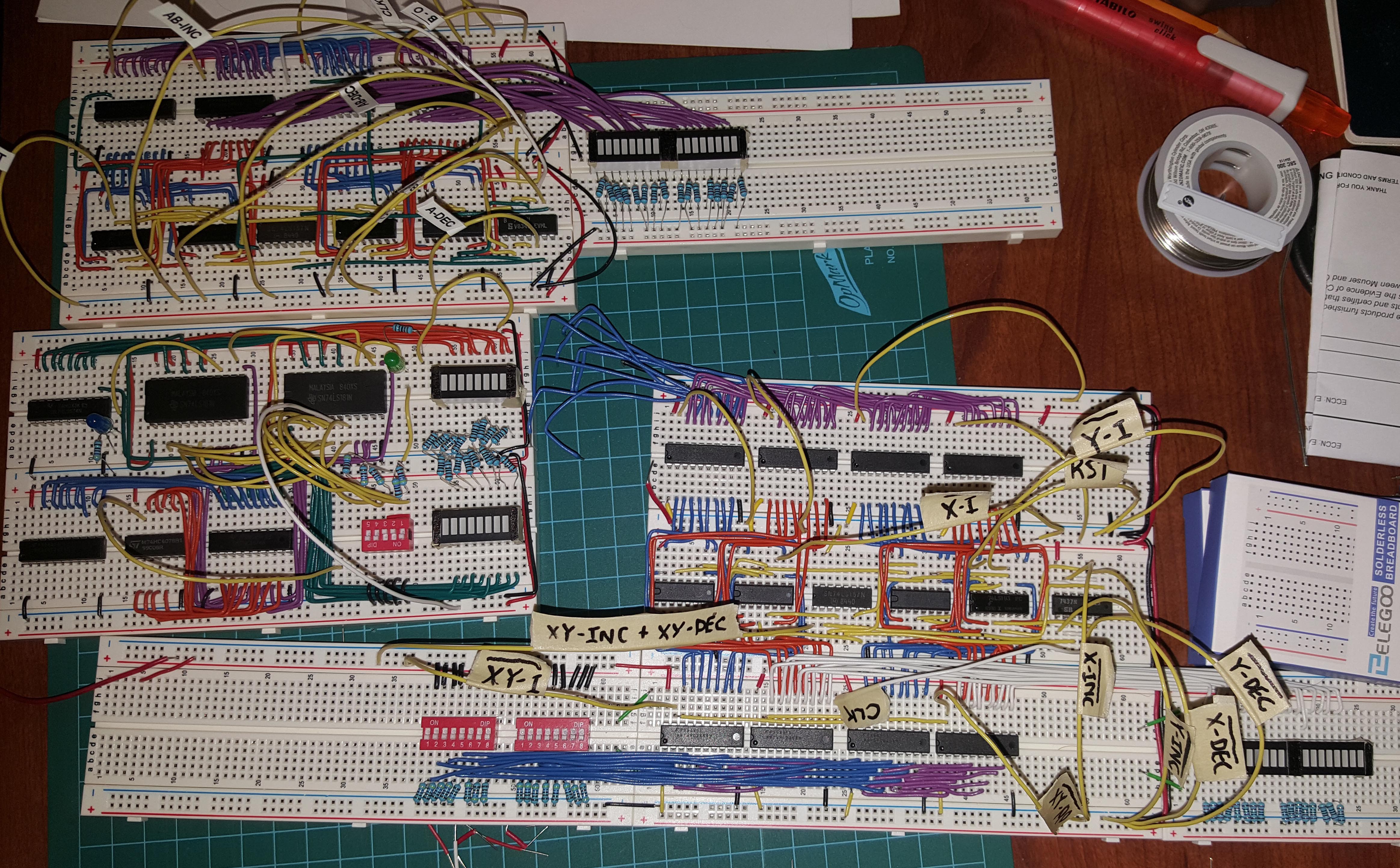 I'm getting enough modules complete to start wiring them all together. I can better judge now how many boards it will take for the whole system. I wish I could buy the power rails separately. I will be needing quite a few for data and address bus.
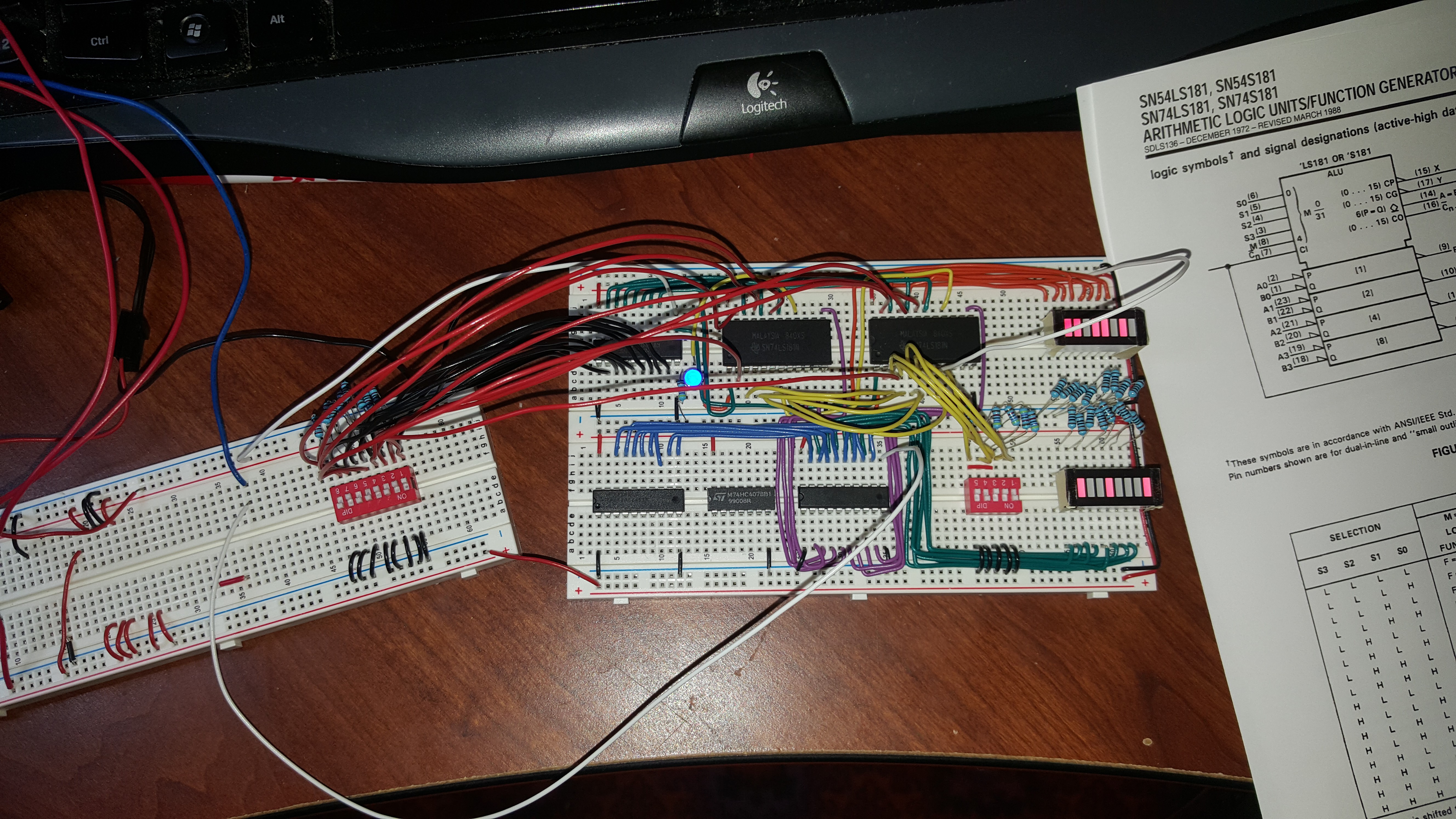


 kaimac
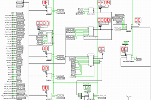
 Ruud van Falier
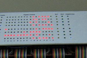
 Pavel
Pavel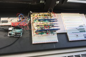
 Jorj Bauer
Great job! It has many similarlies with my breadboard computer.