 spudfishScott
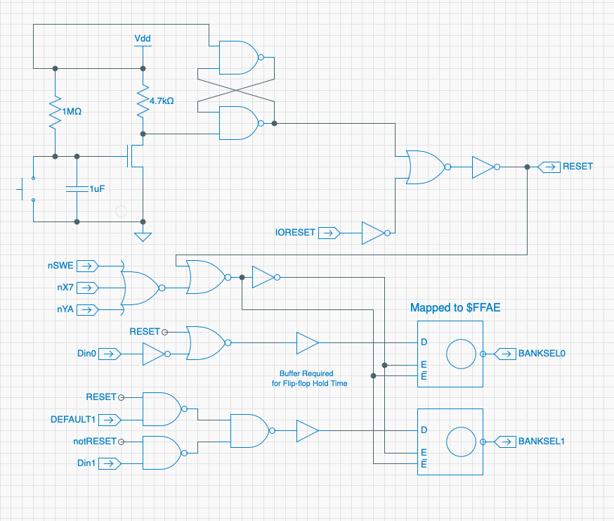
Now that the Spikeputor CPU is up and running, it was time to make some refinements. First up, something that I had been toying with for awhile: replacing the 555s used to generate the clock signal (bistable) and to generate a long RESET signal (monostable). I replaced the monostable 555 circuit with a simple RC circuit. This was incorporated into the start-up schematic that was shown in a previous log. The new version looks like this:
While replacing the bistable 555 circuit for clock signal generation, I reviewed how the Spikeputor writes to memory, as I had been seeing a few glitches in that department. The original design was to trigger the Write Enable signal on the memory chips during the second half of the clock cycle by simply ANDing the inverted clock with the Spikeputor Memory Write Enable (MWE) signal. There were several problems with this approach. First, it gave the Spikeputor only a half a clock cycle to compute the address to write to, effectively limiting the maximum clock cycle frequency. Second, and a bit more concerning, was the fact that there was a possibility that the Write Enable signal might persist while the address bus was changing on the rising edge of the next clock pulse. This could data to get inadvertently written to the wrong location. To avoid cutting it close like that, and to give the Spikeputor more time to compute the address to write to, the following timing was envisioned:

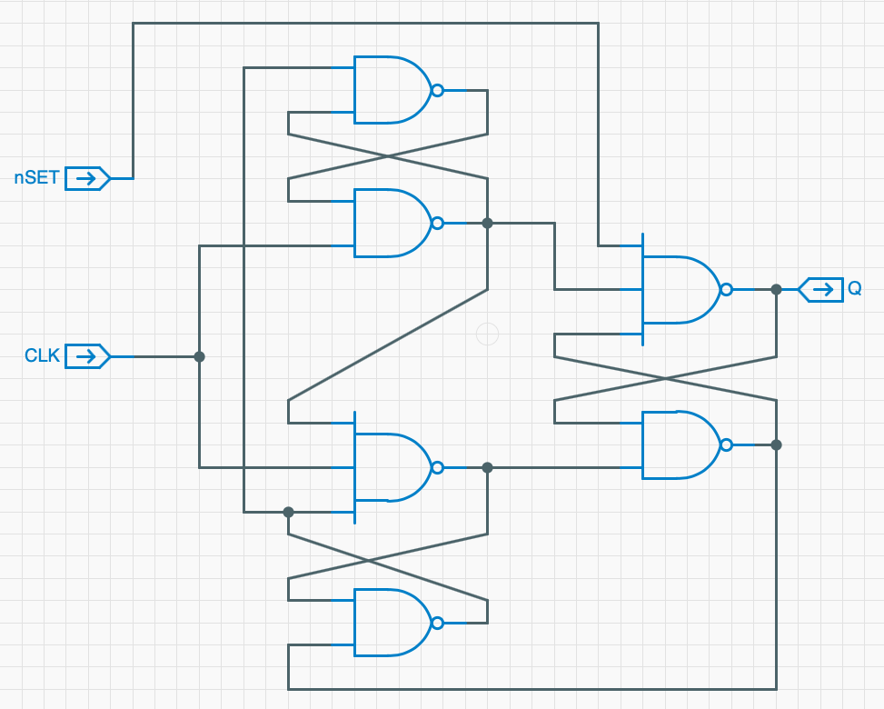
Instead of the Write pulse starting halfway through the clock cycle and ending at the very end, I wanted a pulse that started later and ended before the end of the clock cycle. One relatively easy way to achieve this would be to divide the clock by four and use simple logic gates to generate the desired pulse that starts 3/4 of the way through the cycle and ends 7/8 of the way through. To divide the clock, a discrete Toggle Flip-Flop was designed that toggles its output on every input clock cycle and could also take a SET input, which would be used to reset the new scheme whenever IOFLAG stops the Spikeputor clock:
The discrete 555 circuit was taken from this great kit: https://shop.evilmadscientist.com/productsmenu/652
Putting it all together, the new clock schematic is as follows:
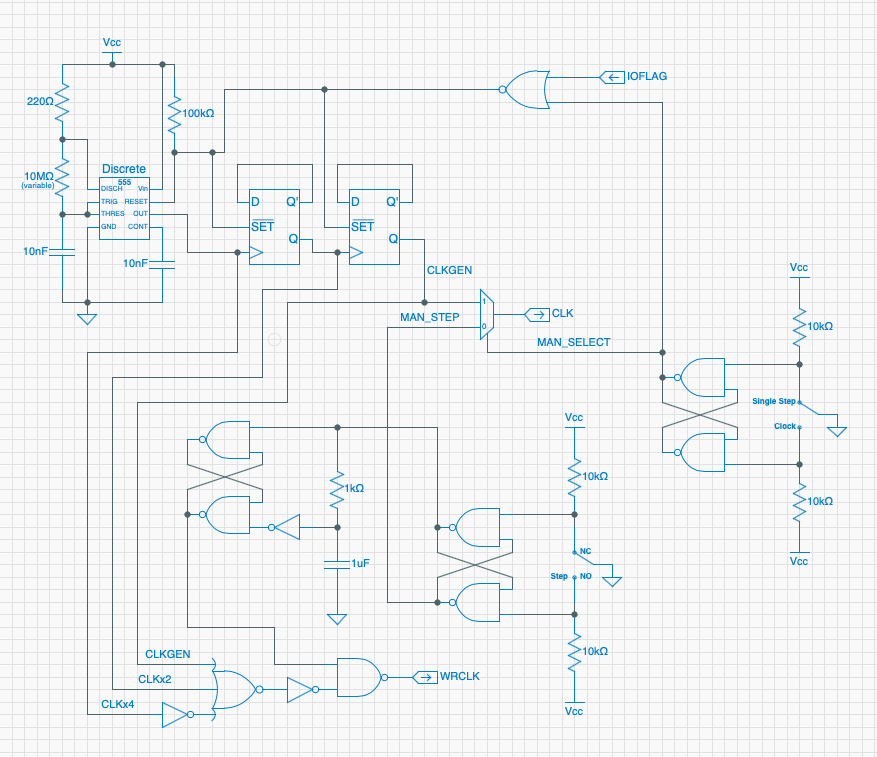
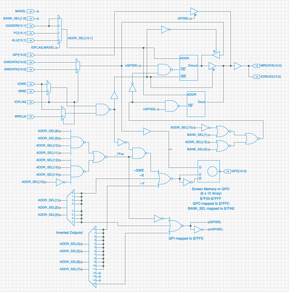
The discrete 555 passes through two T Flip-Flops to divide the signal by 4. The original clock signal and each of the T Flip-Flip outputs are combined via a NOR gate to create the desired proto-signal. This is then OR'd (as created by a NAND with inverted inputs) with a sub-circuit to produce the write pulse a short time after a manual clock pulse, creating the WRCLK signal. That signal in turn replaces the CLK signal input to the memory module, and with a few other small changes to get the phase of the signal right, the new memory schematic is:
Whew! Here's a video of the new clock generator. You can see the clock signal get divided by two twice.
The discrete 555 circuit is on the left half of the board. Measuring 72mm by 48 mm, it is exactly 64 times larger by area than the classic 555 IC package. Cool!
So now the Spikeputor has a new clock, no more 555 chips, and new write signal timing, allowing me to increase the maximum clock frequency by 25%. Next up, time to finish and mount the third pegboard.
Discussions
Become a Hackaday.io Member
Create an account to leave a comment. Already have an account? Log In.