 spudfishScott
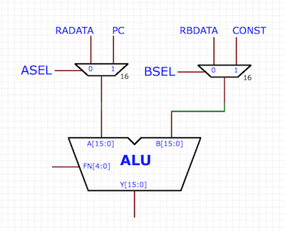
The ALU is the second major module of the Spikeputor, and, including the two input MUX2's, fits neatly on a single pegboard. The design of the ALU again mimics the design of the MITx "Beta" microprocessor. The major differences are the 16 bit (vs. 32 bit for the "Beta") data widths and the fact that, since the opcode width is reduced, the ALU FN input is five bits wide (vs. six). As a result, I needed to take a shortcut with the Boolean module function select (described below). The high-level ALU schematic simply routes the inputs A and B through the four ALU modules and routes the desired function through the function-select MUX4 to the output:
Here's six bits of one of the input MUX2's, placed at the top of the pegboard. The two MUX2's will select between the Register A input and the next PC value (ASEL signal) and between the Register B input and the CONSTANT value (BSEL signal):
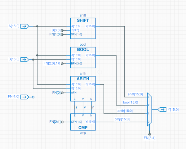
The ARITH module performs addition and subtraction. The heart of the design is a 16 bit ripple carry adder. If AFN (bit 0 of the ALU FN) is 1, the B input is inverted and the initial full adder carry is set to 1. This produces the 2's complement form of the input (B XOR 0xFFFF + 1), and thus, outputs the difference instead of the sum of A and B. There is also logic to determine whether the result is (N)egative, (Z)ero, or caused an o(V)erflow. These flags are used as inputs to the CMP module.

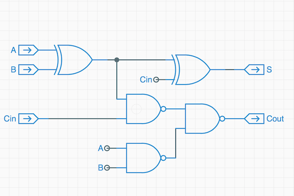
The full adder circuit is standard:
The physical layout of the ARITH function places the B Input inverters directly above the full adder circuitry, keeping all of the bits aligned. This creates some empty space on the inverter breadboards, but greatly simplified the wiring between rows.
Three bits of inverter:
And three bits of full adder:
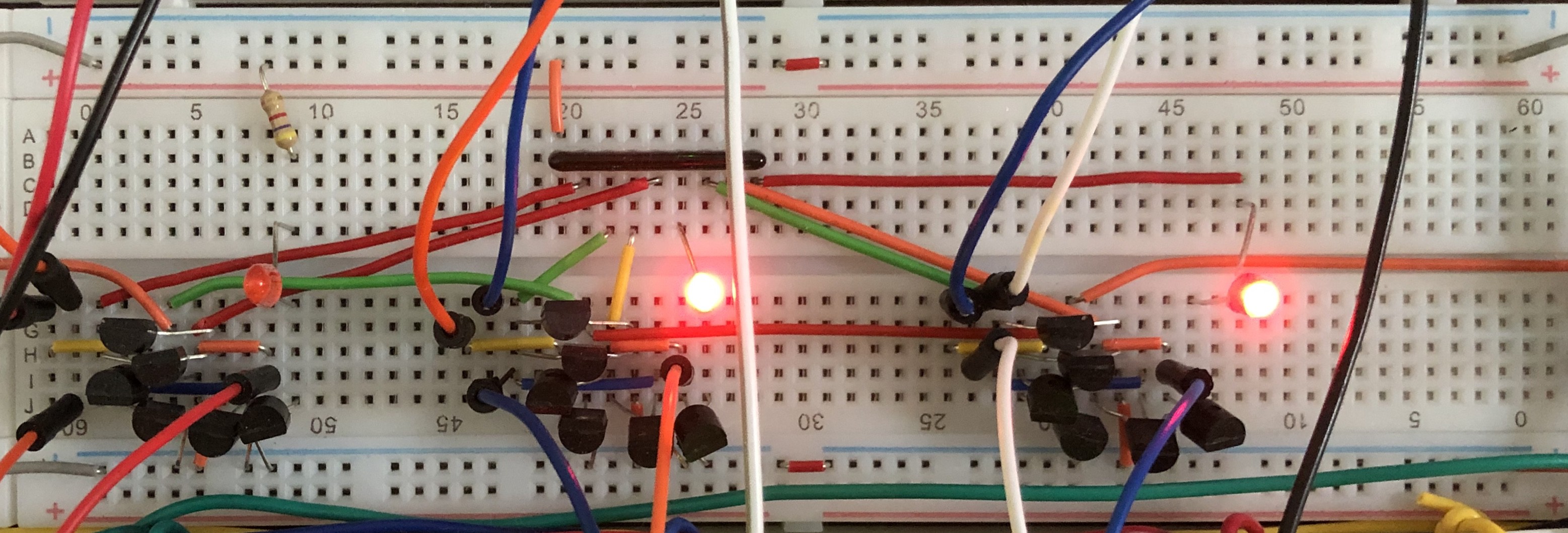
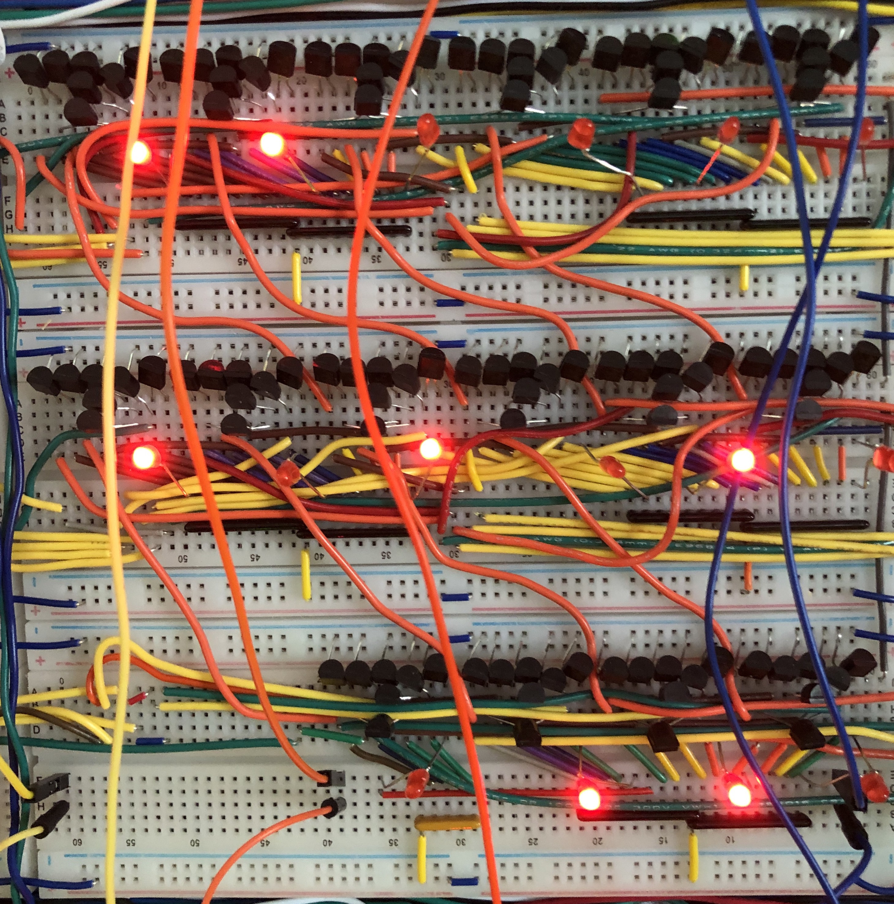
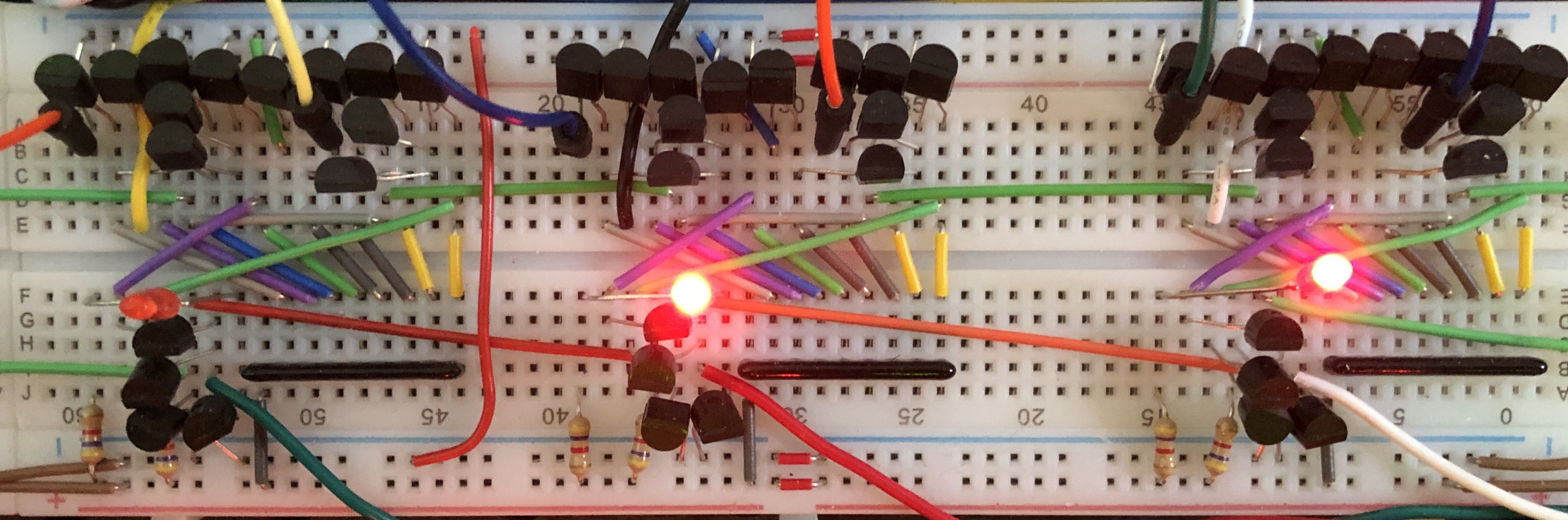
The breadboards used to add and invert the high order bit have extra space on them, and so they conveniently accommodated the N, Z, and V flag logic and the entirety of the CMP module. The CMP circuit just takes A - B from the ARITH modules and looks at those three flags to determine the single bit output based on the value of CFN (bits 1 and 2 of the ALU FN):

The BOOL module provides bitwise logic operations between the two inputs. Each bit of the module simply combines the A and B inputs to create a two bit select signal for a MUX4. The four inputs of the MUX then correspond to the truth table for each pair and A and B bits. In the original "Beta" design, each of these four values was directly taken from the ALU FN, allowing for instructions that can create any two-input logic function. Because I only had five bits to use for the entire ALUFN, and two of those ware used to select which module to output, I was forced to make do with the remaining three bits for the BFN input. Luckily, all of the major logic functions I wanted to implement (AND, OR, XOR, and A Identity) can be produced with three bits, hard-wiring channel 0 of the MUX4 to 0.
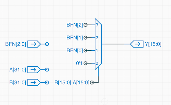
To produce an AND function, BFN is 0b100. OR is 0b111, XOR is 0b011, and the A Identity function is 0b101.
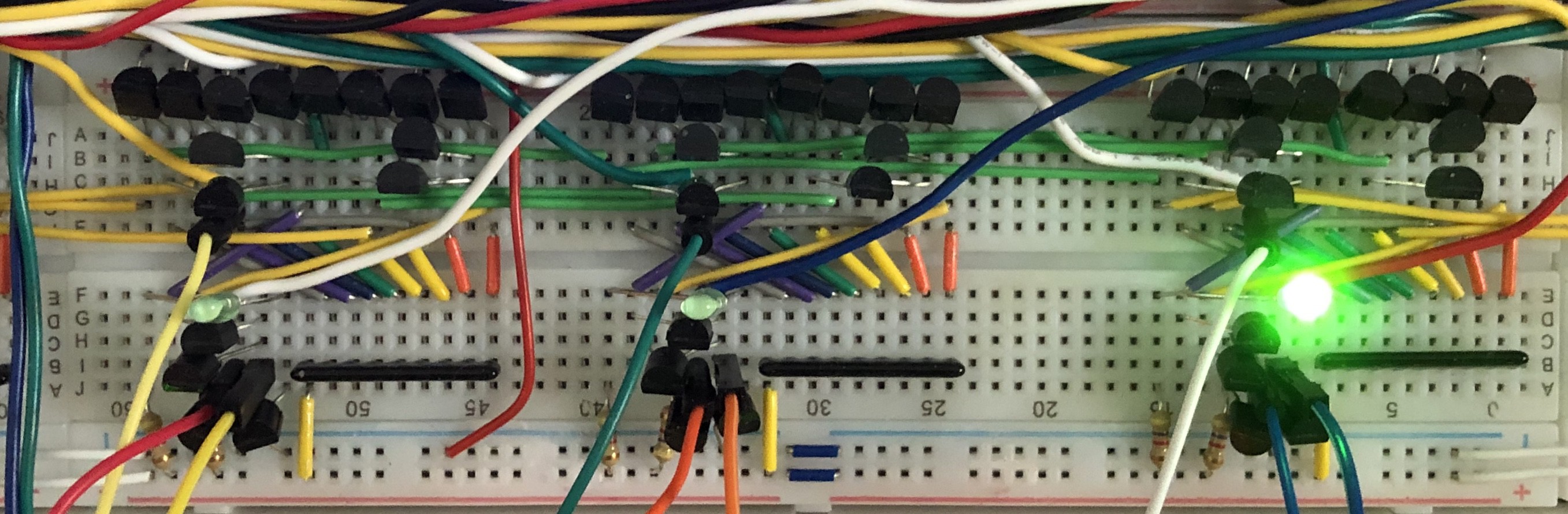
Three bits of BOOL:
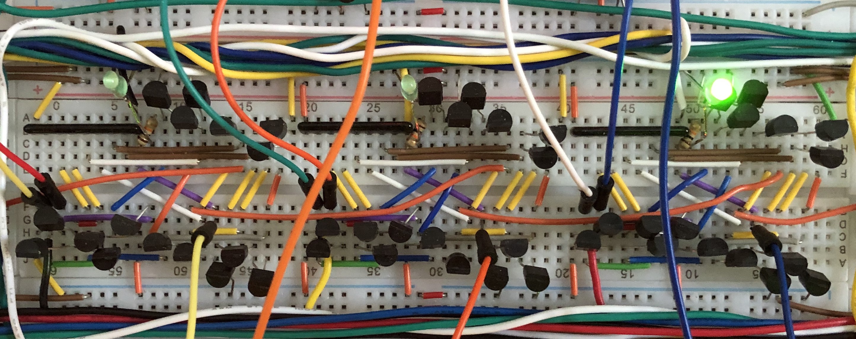
The SHIFT module is considerably more complicated. It takes the lower four bits of Input B to determine how many bits to shift Input A. Depending on the SFN inputs, the bits are shifted to the left or right, and with or without sign-extending bit 15. The sub-module is implemented with a cascade of six MUX2's. Four MUX2's shift the number 1, 2, 4, or 8 bits to the left or allow it to simply pass through, depending on the value of Input B. The remaining two MUX2's reverse the bit order of Input A and reverse it back after the shift operations in order to procedure right-shifted results:

The physical layout of the SHIFT module breaks with the usual one row per word design, instead placing each of the MUX2's in a single column that is three rows tall. Here's one column of the SHIFT module, which corresponds to all 16 bits of the SHIFT4 MUX2 in the schematic:
The output of each module is directed to a MUX4 to select the ALU output. These boards are physically below all of the other ALU modules:
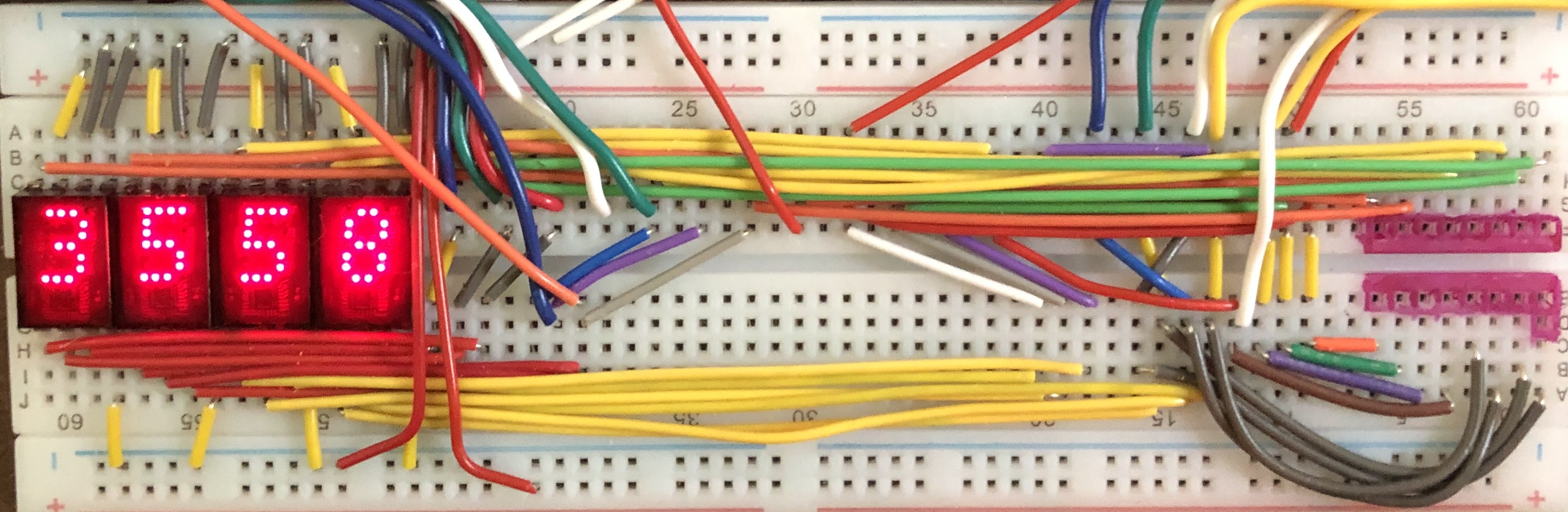
Finally, at the very bottom of the pegboard is the ALU Output board, which features a numeric display and an area for a 16-pin ribbon cable to direct the ALU Output to the rest of the CPU:
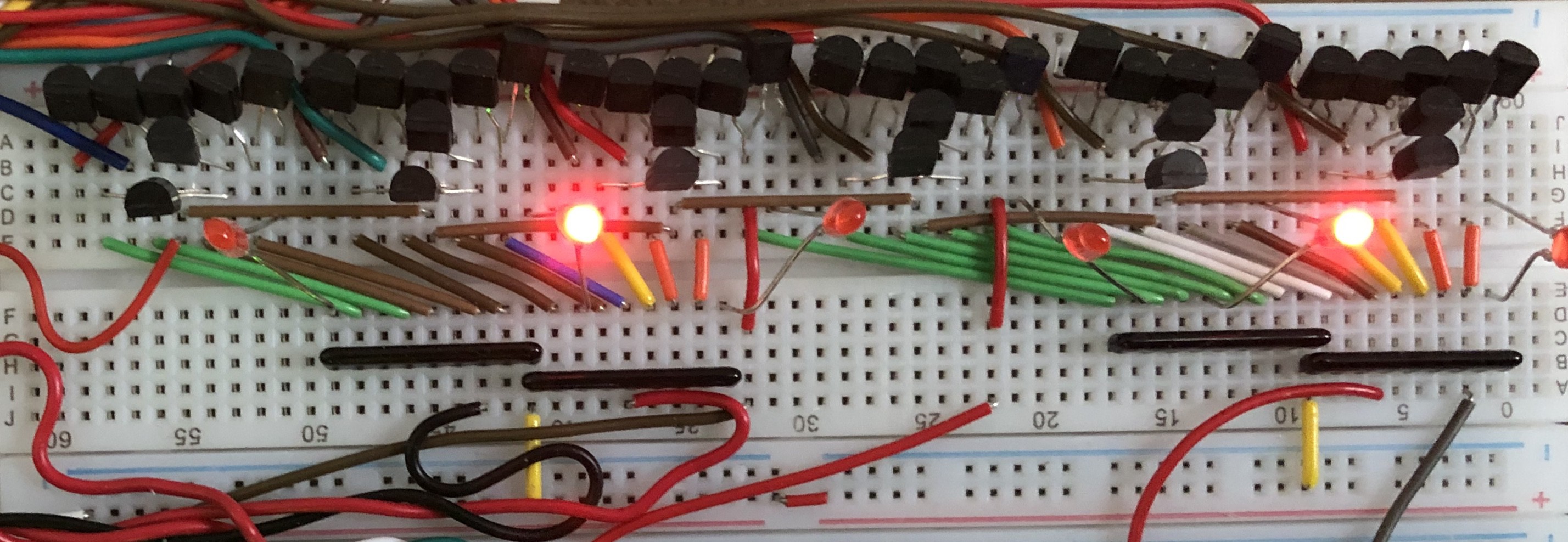
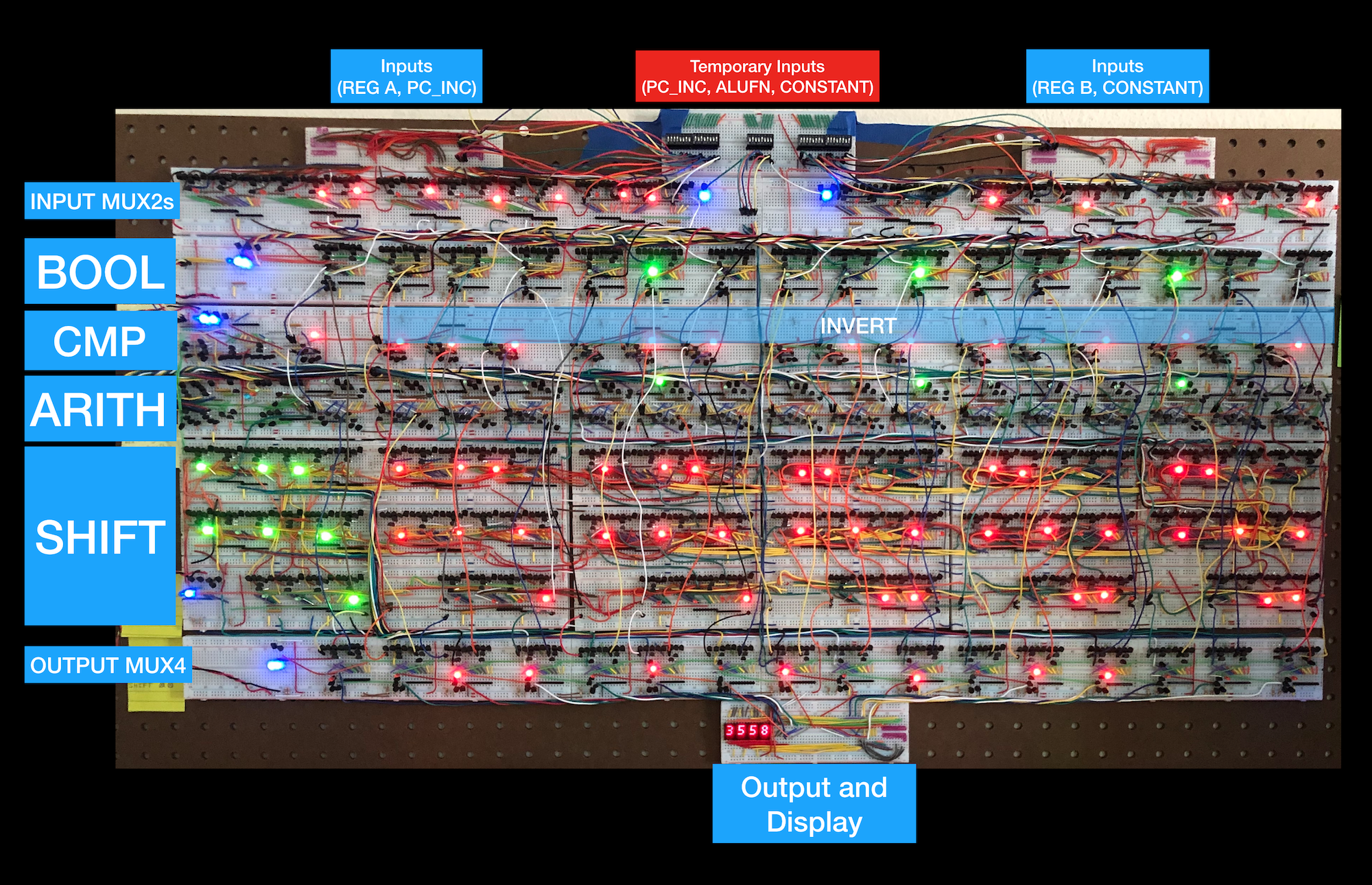
Putting everything together, here's the entire ALU pegboard, annotated:
Discussions
Become a Hackaday.io Member
Create an account to leave a comment. Already have an account? Log In.