 spudfishScott
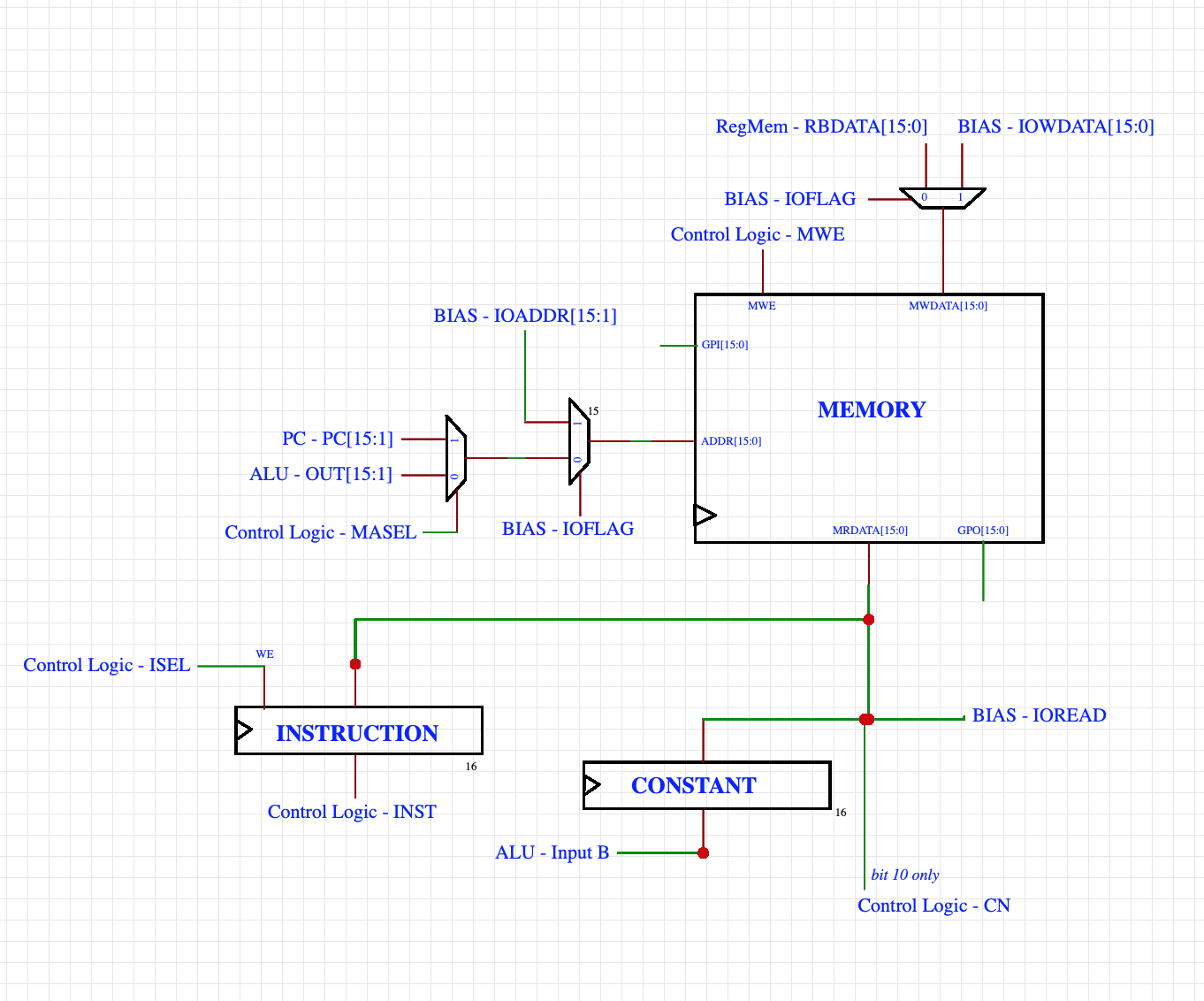
The Spikeputor memory module consists of two channels to address and read/write memory. One channel allows the CPU to access memory, and the other is used for DMA functions. The CPU can address memory from the Program Counter or from the ALU ouput, depending on the value of the MASEL (Memory Address SELect) signal. The DMA functions are performed by the BIAS card on the Apple II. Bringing the IOFLAG signal high pauses the CPU clock and redirects all memory access to BIAS. The memory is written to when either the MWE signal is high (set during the CPU STore command) or when the BIAS card sets IOW high. Memory data is available to be read by the CPU or BIAS as long as MWE (Memory Write Enable) is low. When high, MRDATA is undefined (high-Z). Memory data is stored in INSTRUCTION and CONSTANT registers as appropriate (discussed in the previous log entry). Additionally, bit 10 of the Memory data output is wired directly to the CN (Constant Needed) signal of the CPU Control Logic.
In addition to DMA, there are 16 bits of General Purpose Input and 16 bits of General Purpose Output. These are hard coded to memory location $FFFE and can be written to in order to set the GPO lines and read from in order to read the GPI lines regardless of the current settings of the RAM/ROM Bank Select (see below).
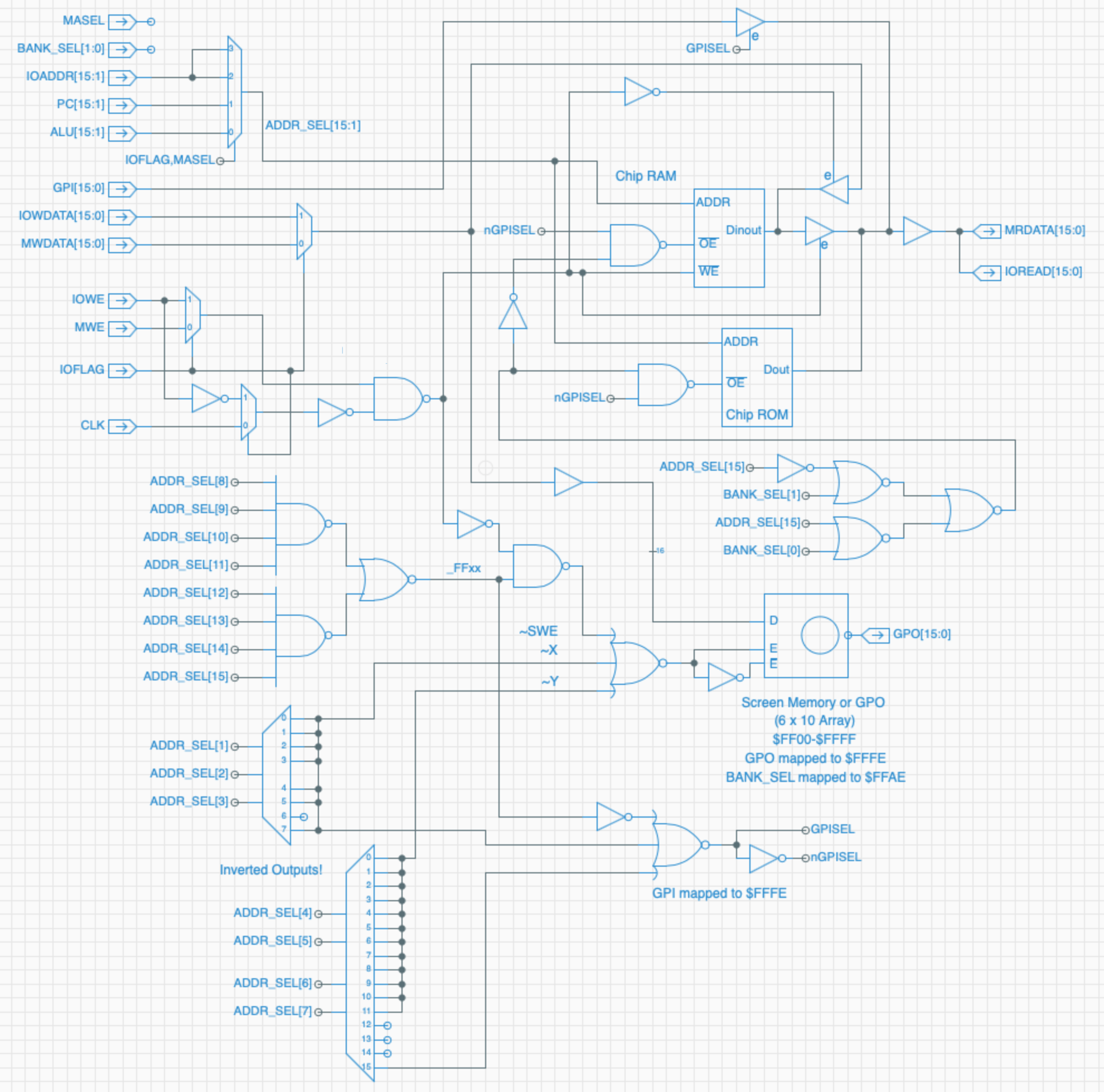
Memory storage is implemented in two ways. First, there are 32K words each of RAM and ROM, implemented by two each of 32K x 8 bit Static RAM (AS6C62256) and PROM (AT27C256R) chips. While RAM is always written to, whether RAM or ROM is read from depends on a bank-selection scheme, controlled by a two-bit specialty register, BANK_SEL. The value of BANK_SEL is set by writing the desired lower two bits to memory location $FFAE. RAM and ROM banks are accessed as shown in the table below:
| BANK_SEL[0] = 0 | BANK_SEL[0] = 1 | |
| BANK_SEL[1] = 0 | RAM: $0000-$FFFF | ROM: $0000-$7FFF RAM: $8000-$FFFF |
| BANK_SEL[1] = 1 | (default) RAM: $0000-$7FFF ROM: $8000-$FFFF | ROM: $0000-$FFFF |
Second, there will eventually be 54 words of memory made via discrete transistors, resistors and LEDs, laid out to produce a 48 x 18 array of "screen memory" (this will be the last thing completed for the main Spikeputor boards). This memory will be "write-only," and will mirror chip RAM in the range $FF00-$FFFF.
The schematic of the memory modules is as follows:
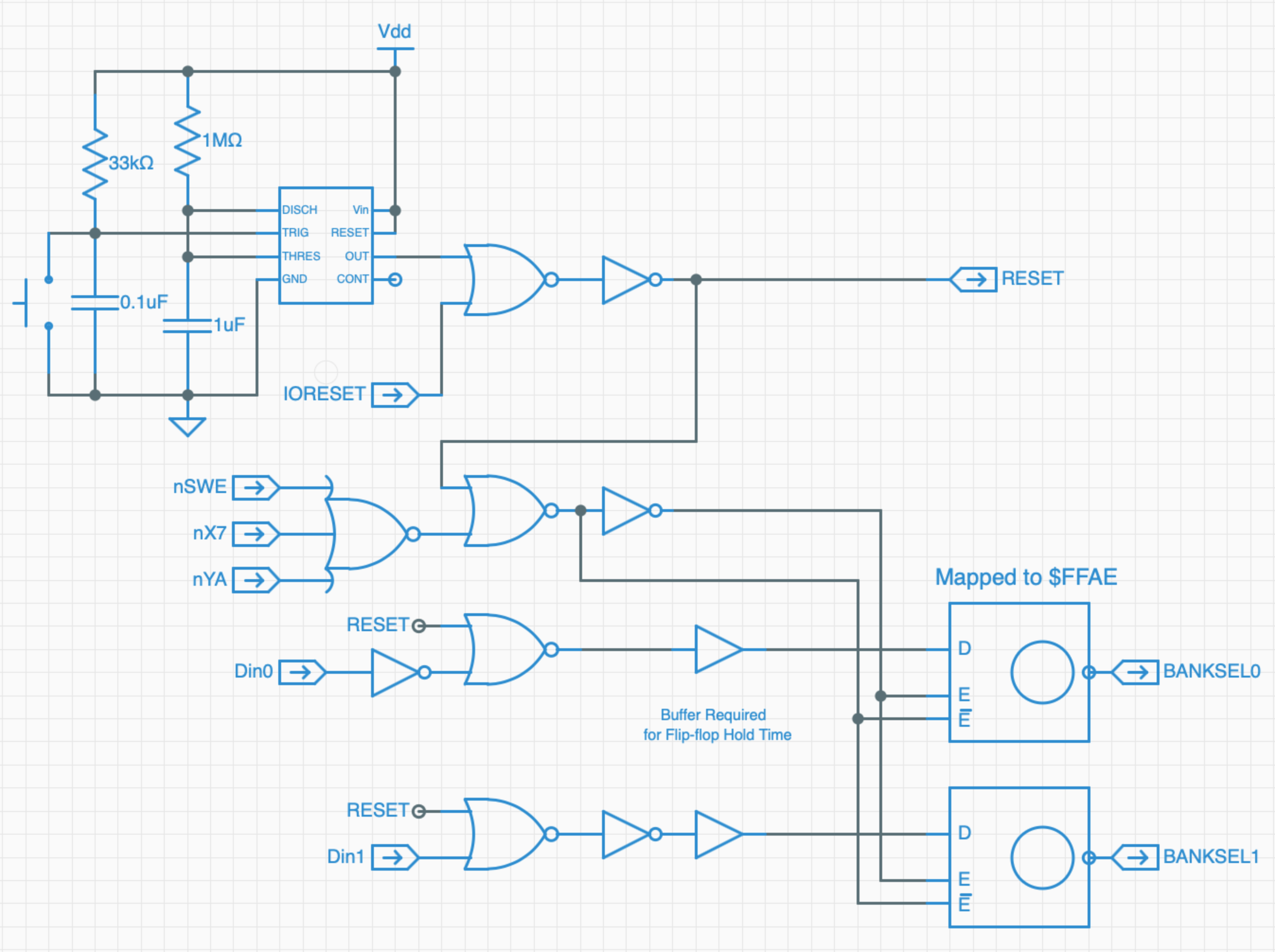
Finally, the power-up/reset logic is implemented via the following schematic. A RESET signal is simulated upon power-on and can be set manually via a debounced pushbutton or set via the BIAS card IORESET signal. RESET restores the BANK_SEL values to their defaults (0b10). The implementation of the simple memory elements for BANK_SEL was discussed in the "Building Blocks" section of the logs.
Here's a photo of the actual Memory Module, followed by a block diagram of everything that's going on.
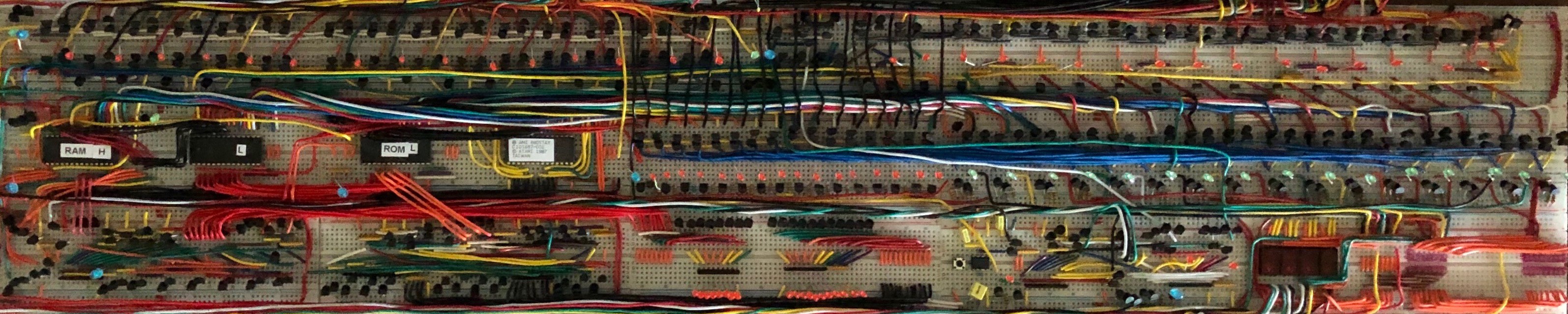
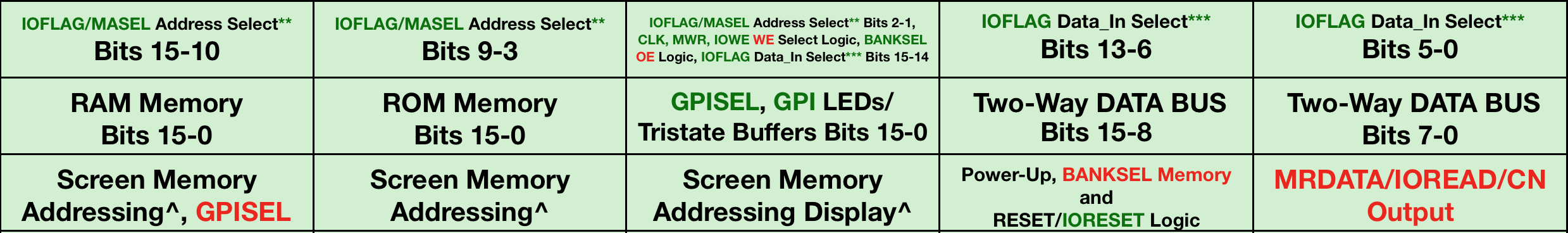
The top row handles the selection of address and data input based on the logic described above, implemented by a pair of MUX2's for address input and a single MUX2 for data input. The next row contains the actual RAM and ROM chips, the general purpose input logic and LED display, and the data bus. Finally, the third row contains the screen memory addressing logic (a 3 to 8 decoder and a 4 to 16 decoder, partially implemented) and display, the power-up/reset/bank_sel logic, and a numeric display and output ports for the memory data output.
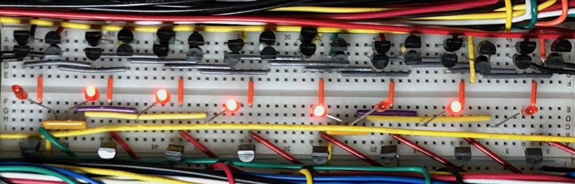
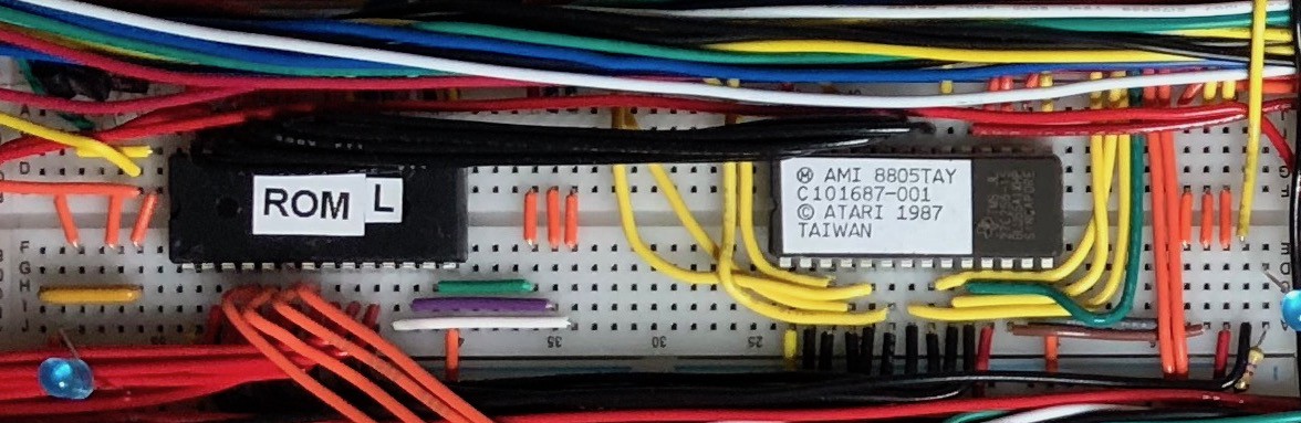
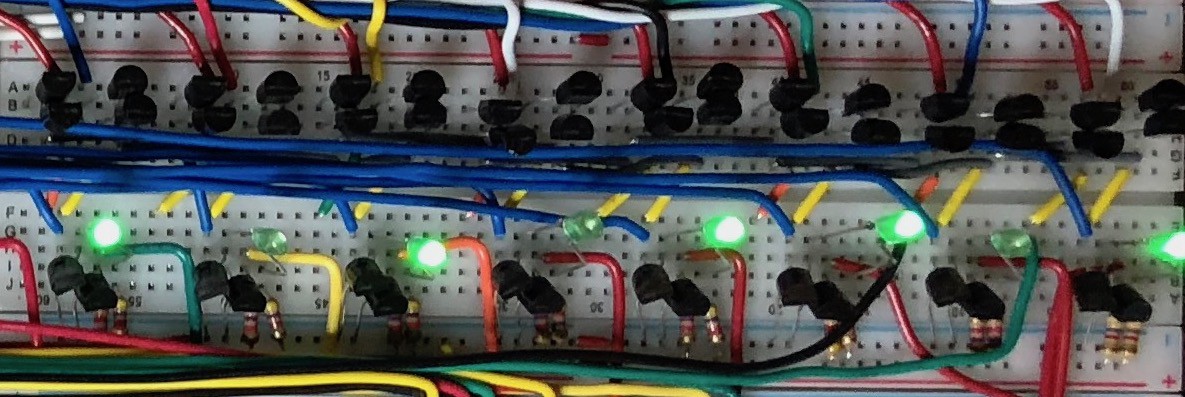
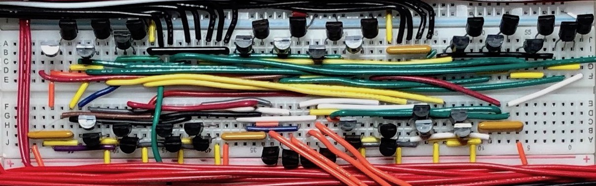
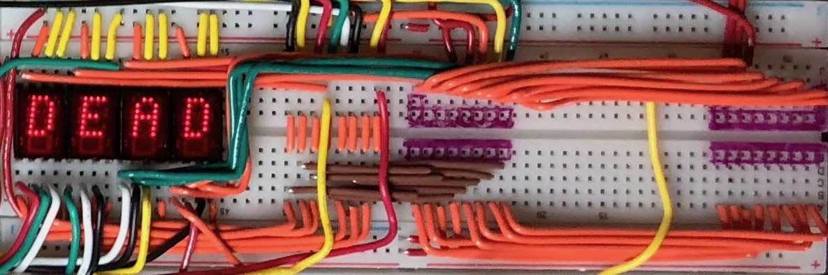
Detailed photos of individual breadboards follow.
Six bits of the address select logic:
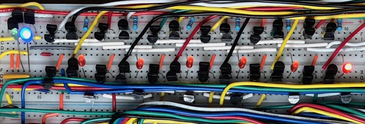
Eight bits of the data_in select logic:
RAM Chip Memory:

ROM Chip Memory (including an old Atari ROM chip for testing):
Eight bits of the Data Bus:
The 4 to 16 decoder for screen memory addressing, decoding the third nybble of the address. Only 11 lines are implemented since there are only nine rows of screen memory ($FF[0...9]x), plus one each to address BANK_SEL ($FF[A]E) and general purpose inputs and outputs ($FF[F]E).
The power-up/reset/bank_sel board:

And finally, the Memory Data Output board, displaying one of my favorite hex numbers:
Next up: building the INSTRUCTION and CONSTANT registers, and then the Program Counter logic to complete the CPU!
Discussions
Become a Hackaday.io Member
Create an account to leave a comment. Already have an account? Log In.