 spudfishScott
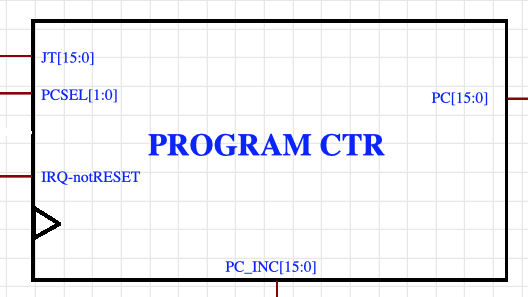
The final module to add to the core Spikeputor CPU is the program counter. The PC inputs are a JT (Jump to...) Address, a two bit PC Select (PCSEL) signal, and a signal to distinguish between a RESET or IRQ (IRQ-notRESET). Outputs are the current PC address, used to read the next instruction from memory, and the current PC address incremented by two bytes (one word), used to calculate branch offsets or to store a return address to a selected register.
The schematic of the program counter includes a MUX4, a D-Register to store the PC output value on the next clock pulse, and a half adder with the initial input carry set to 1 to increment the current PC output value. Since the Spikeputor design restricts all memory access to even boundary addresses, the MUX4, register, and half adder circuits are only 15 bits wide with the lowest significant bit of the outputs hard coded to zero. The PCSEL signal input to the MUX4 selects which of four values is latched into the PC Register on the next clock pulse.
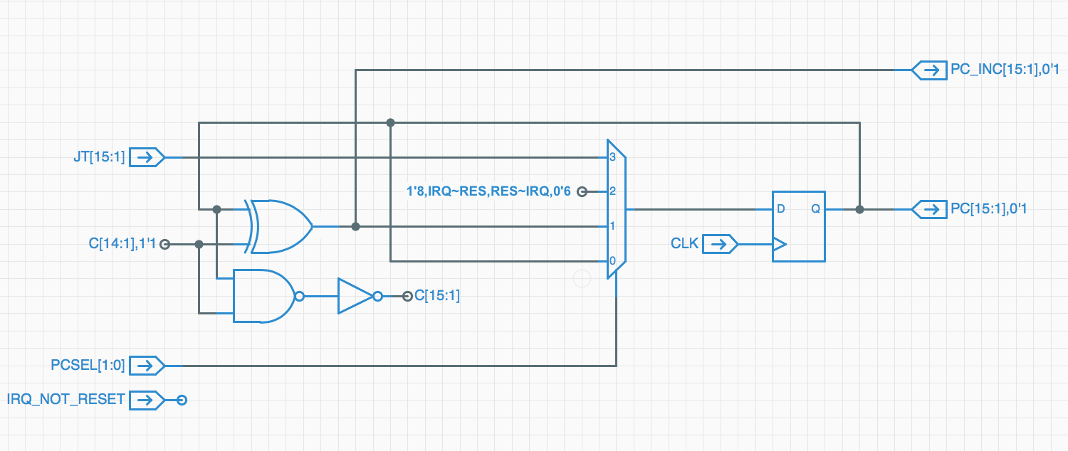
When PCSEL is 0, the current value of the PC is retained on the next clock pulse.
A PCSEL signal of 1 selects the output of the half adder, incrementing the current PC address.
With a value of 2, the next PC value is set to either the RESET ($FFD0) vector or the IRQ vector ($FFE0).
Finally, a PCSEL value of 3 indicates that the JT input should be the next PC value, enabling branching.
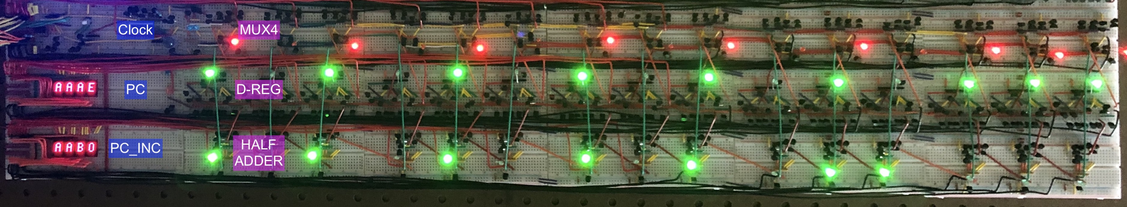
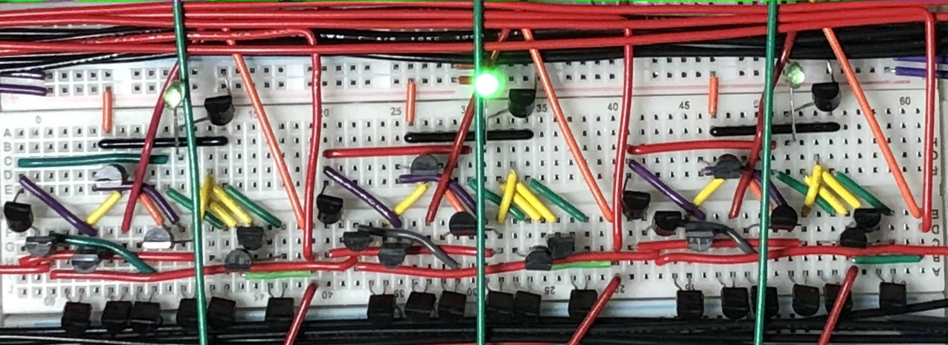
The entire Program Counter module is shown below. The clock board for the CPU is also pictured, since there was one open space for it to conveniently be placed.
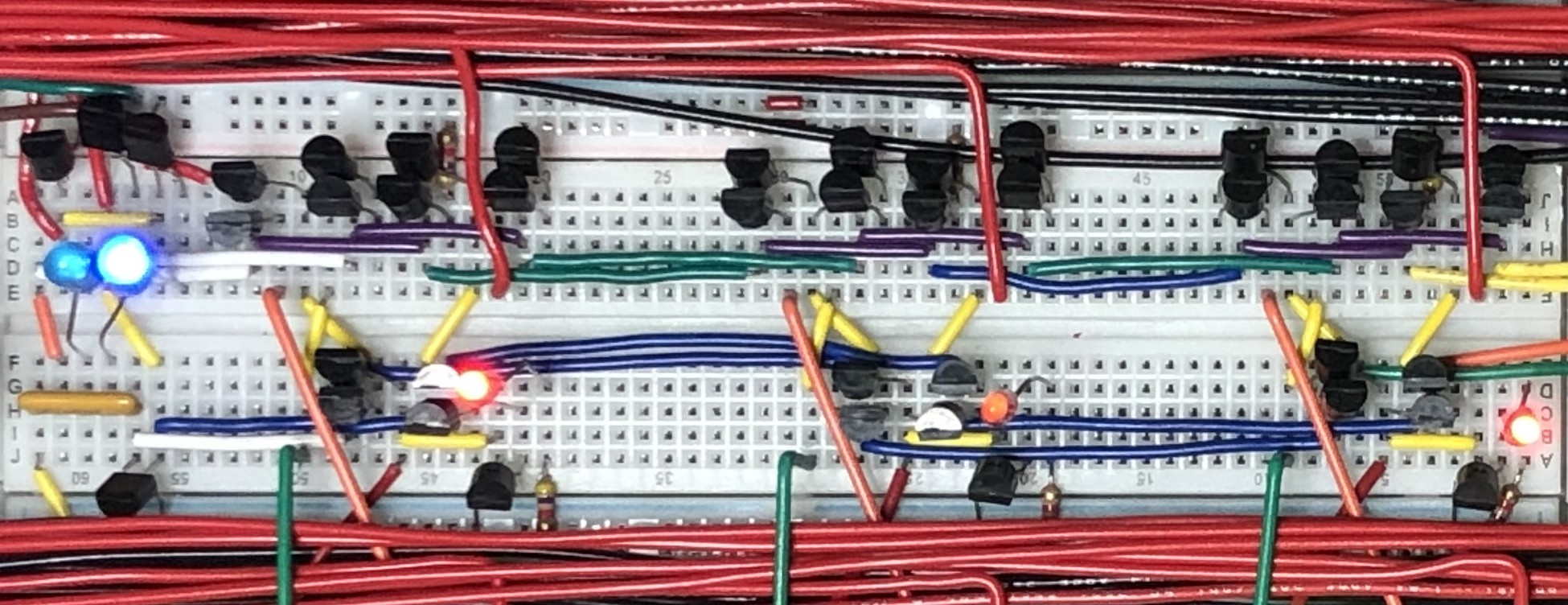
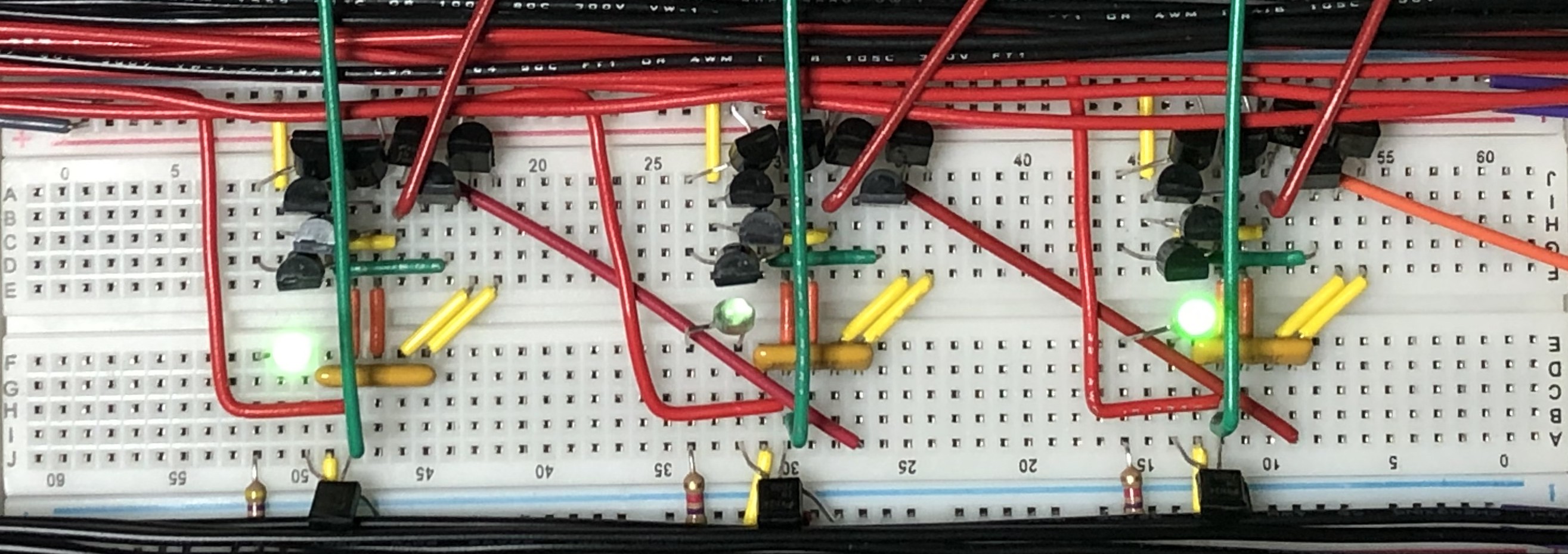
Here's a close-up of three MUX4 bits. The two blue LEDs reflect the PCSEL signal:
And three bits of the PC Register:
Finally, three bits of the half adder:
To test the PC module, I applied the clock signal and manipulated the PCSEL signal to simulate the CPU under different conditions.
Initially, the PCSEL signal switches between 1 and 0 to simulate CPU phases 0 and 2, where an instruction is read, the PC is held constant, and the instruction is executed on the next clock pulse as the PC is incremented to fetch the next instruction.
Later (at 0:16), I simulated a RESET condition. The PCSEL signal goes to 2, which sets the next PC value to the RESET vector, $FD00. From there, the cycle above continues from that address.
Finally (at 0:34), by manipulating the control signals to simulate a JMP instruction, PCSEL goes to 3, which sets the program counter to a (hard-coded for this test) new address to continue the fetch-execute cycles.
With the PC module complete, it remains to integrate all of the modules and start testing out actual programs! There are still a few major additions to complete as well (screen memory, logic path illumination), but those will be additions to the functional CPU. Stay tuned!
Discussions
Become a Hackaday.io Member
Create an account to leave a comment. Already have an account? Log In.