spudfishScott
-
Adding the Program Counter Completes the Core CPU!
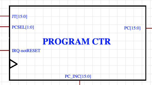
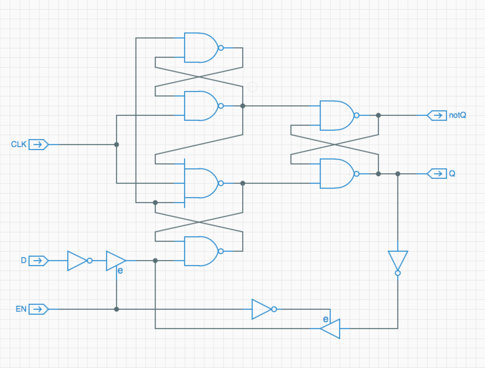
11/05/2019 at 17:20 • 0 commentsThe final module to add to the core Spikeputor CPU is the program counter. The PC inputs are a JT (Jump to...) Address, a two bit PC Select (PCSEL) signal, and a signal to distinguish between a RESET or IRQ (IRQ-notRESET). Outputs are the current PC address, used to read the next instruction from memory, and the current PC address incremented by two bytes (one word), used to calculate branch offsets or to store a return address to a selected register.
![]()
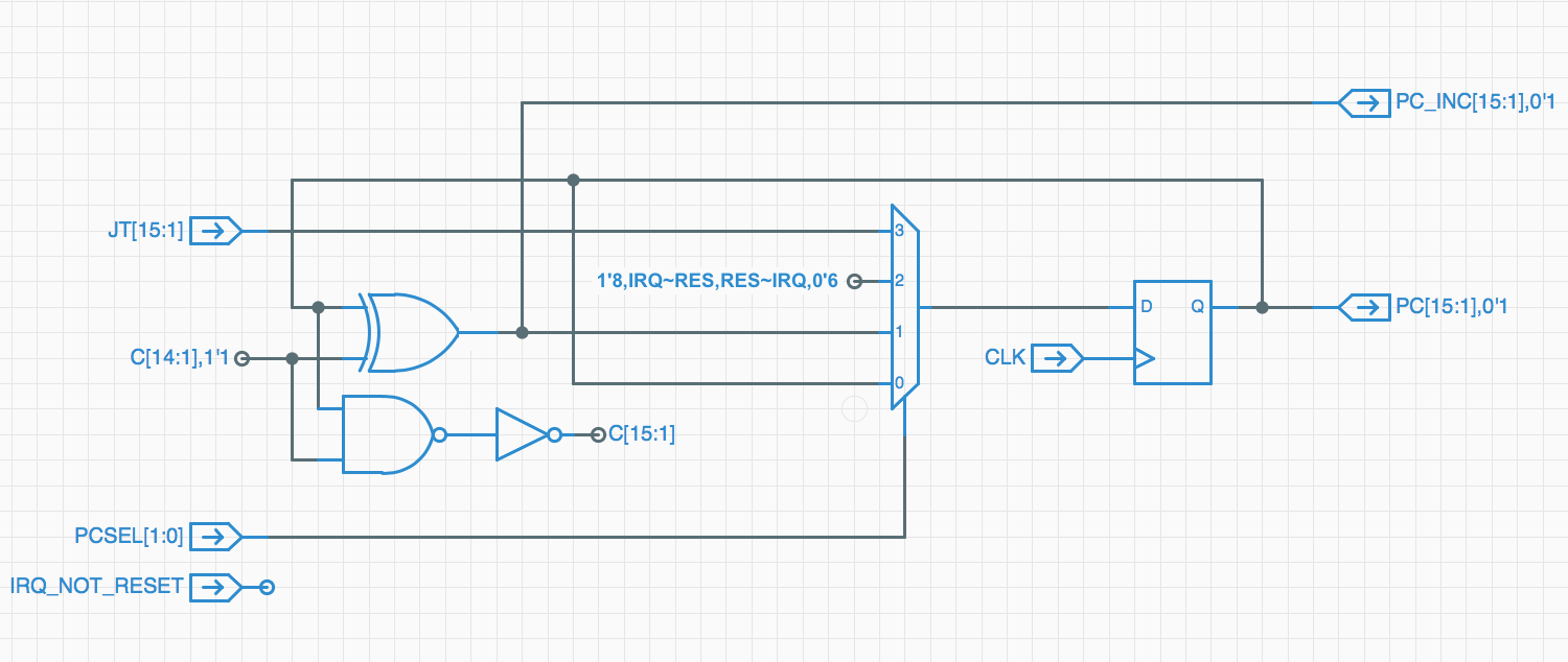
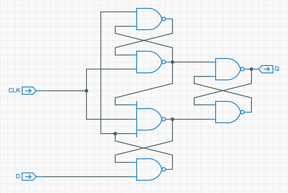
The schematic of the program counter includes a MUX4, a D-Register to store the PC output value on the next clock pulse, and a half adder with the initial input carry set to 1 to increment the current PC output value. Since the Spikeputor design restricts all memory access to even boundary addresses, the MUX4, register, and half adder circuits are only 15 bits wide with the lowest significant bit of the outputs hard coded to zero. The PCSEL signal input to the MUX4 selects which of four values is latched into the PC Register on the next clock pulse.
![]()
When PCSEL is 0, the current value of the PC is retained on the next clock pulse.
A PCSEL signal of 1 selects the output of the half adder, incrementing the current PC address.
With a value of 2, the next PC value is set to either the RESET ($FFD0) vector or the IRQ vector ($FFE0).
Finally, a PCSEL value of 3 indicates that the JT input should be the next PC value, enabling branching.
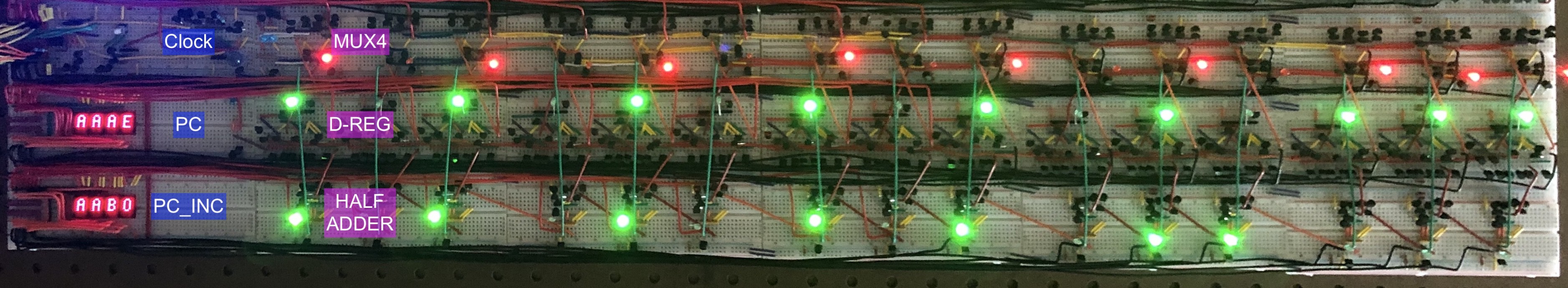
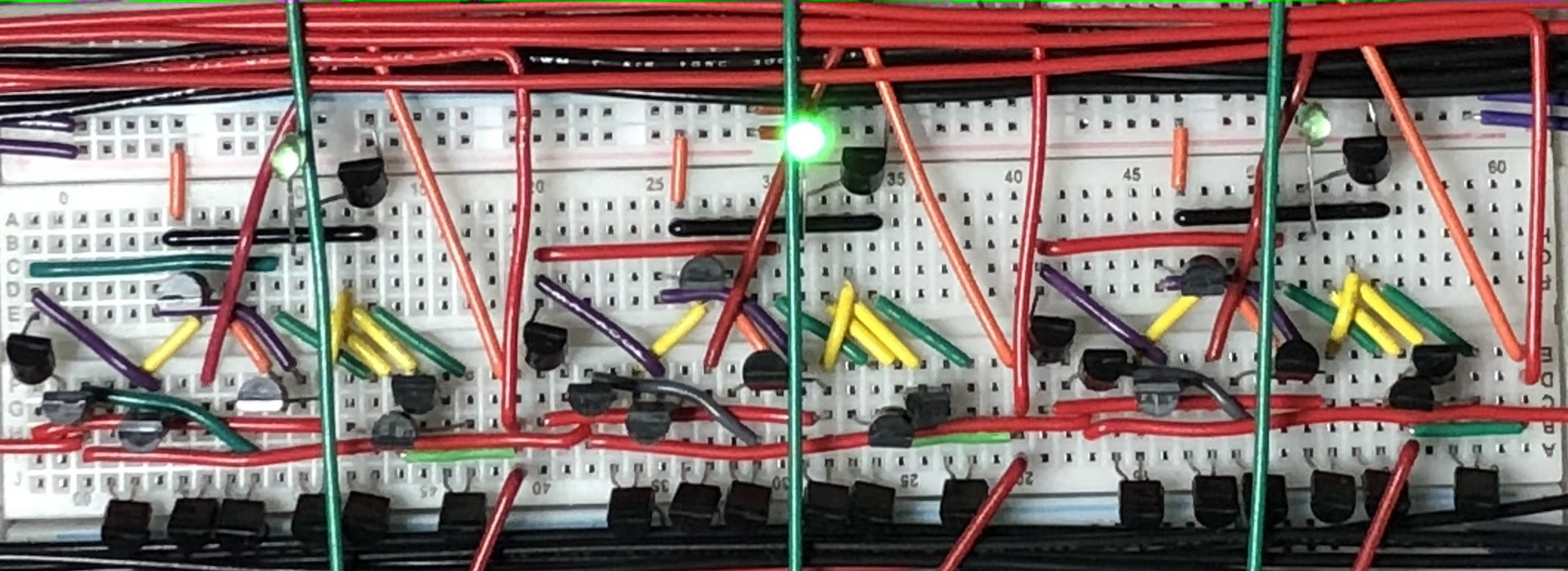
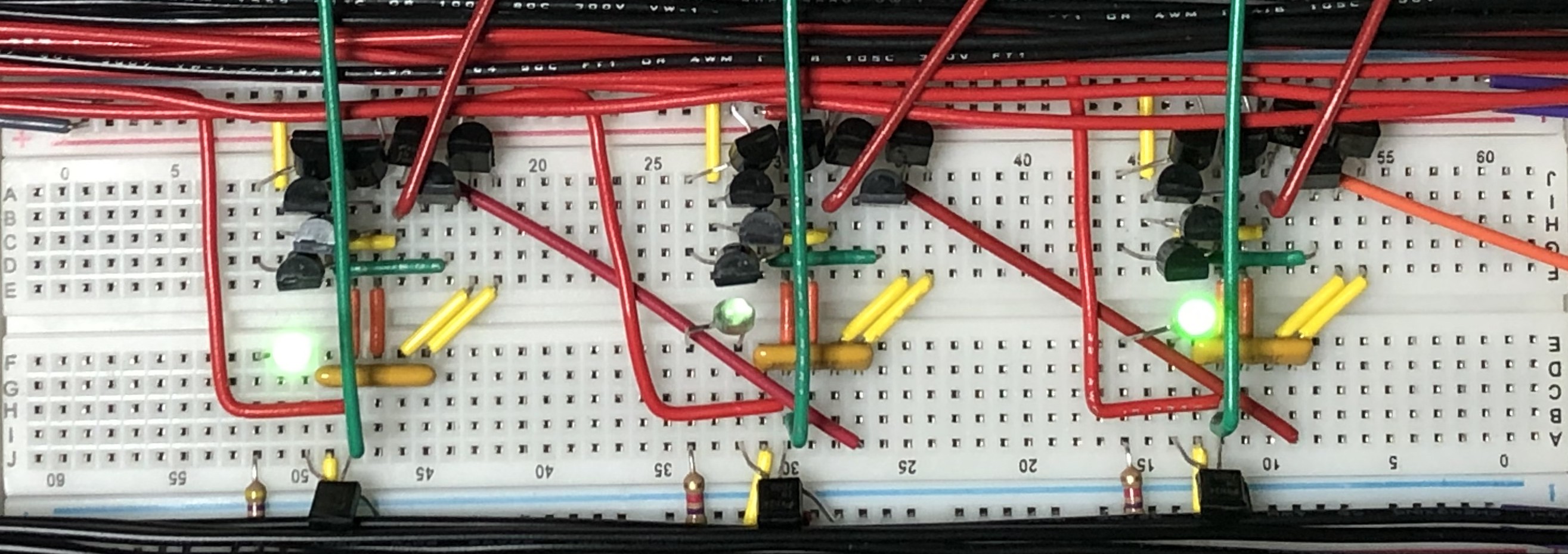
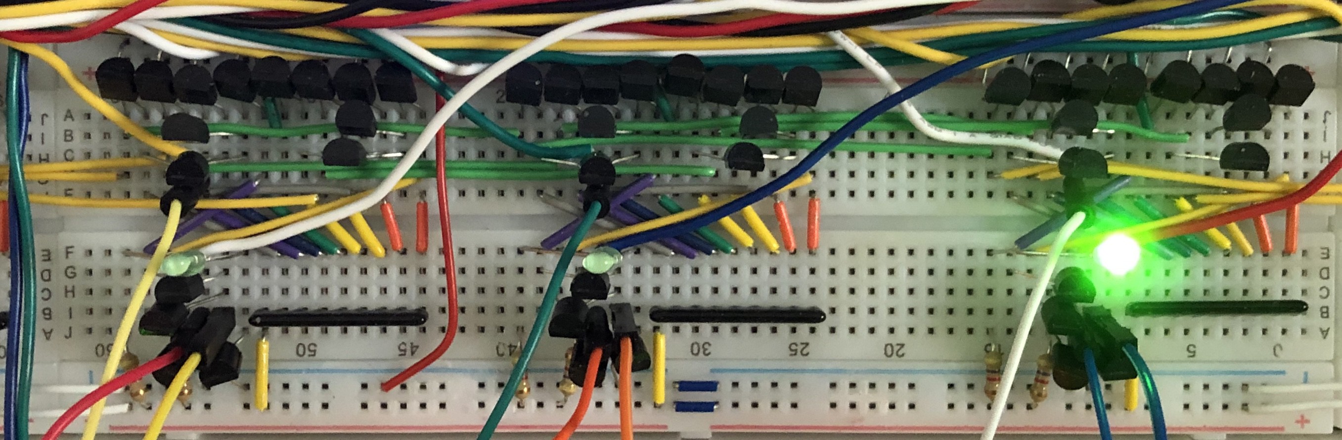
The entire Program Counter module is shown below. The clock board for the CPU is also pictured, since there was one open space for it to conveniently be placed.
![]()
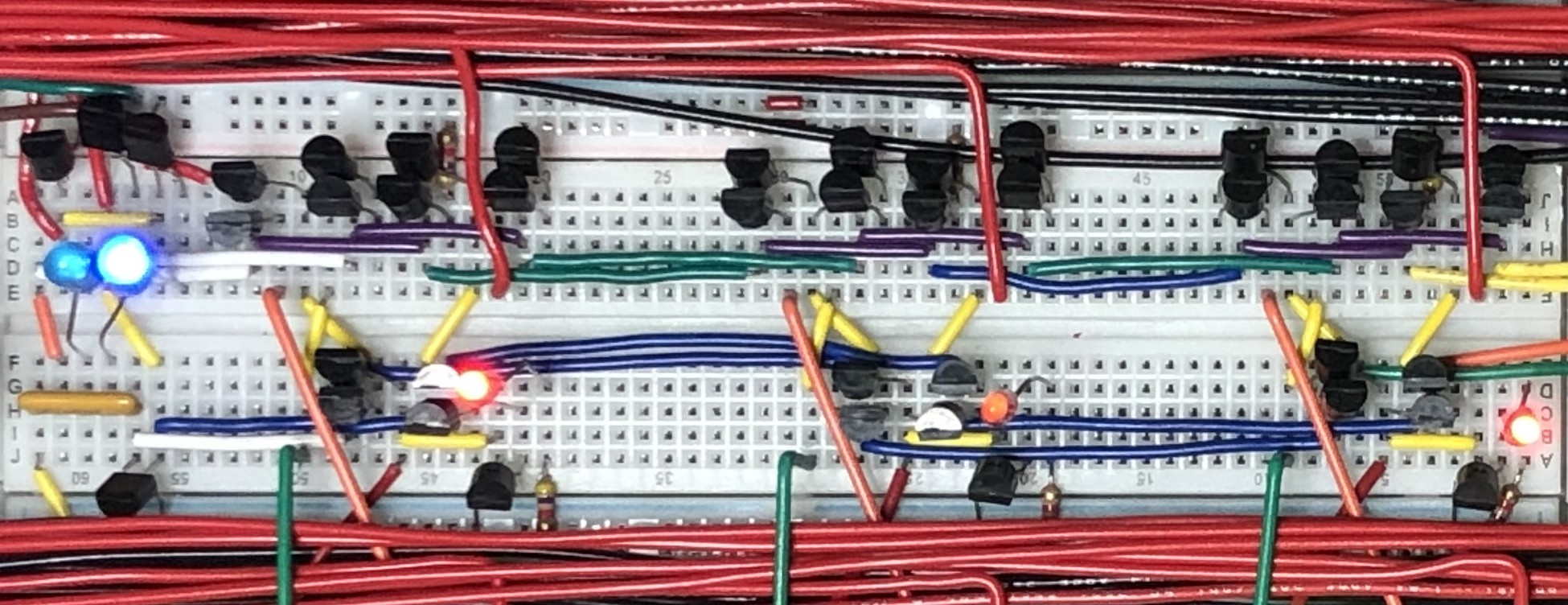
Here's a close-up of three MUX4 bits. The two blue LEDs reflect the PCSEL signal:
![]()
And three bits of the PC Register:
![]()
Finally, three bits of the half adder:
![]()
To test the PC module, I applied the clock signal and manipulated the PCSEL signal to simulate the CPU under different conditions.
Initially, the PCSEL signal switches between 1 and 0 to simulate CPU phases 0 and 2, where an instruction is read, the PC is held constant, and the instruction is executed on the next clock pulse as the PC is incremented to fetch the next instruction.
Later (at 0:16), I simulated a RESET condition. The PCSEL signal goes to 2, which sets the next PC value to the RESET vector, $FD00. From there, the cycle above continues from that address.
Finally (at 0:34), by manipulating the control signals to simulate a JMP instruction, PCSEL goes to 3, which sets the program counter to a (hard-coded for this test) new address to continue the fetch-execute cycles.
With the PC module complete, it remains to integrate all of the modules and start testing out actual programs! There are still a few major additions to complete as well (screen memory, logic path illumination), but those will be additions to the functional CPU. Stay tuned!
-
Special Registers Completed
10/12/2019 at 22:54 • 0 commentsSince I've been away from the Spikeputor Manufacturing Center in Texas, it's been awhile since I've been able to make any progress on the project. I finally got there and spent some time completing the last two items referenced in the Memory Module. These are two special 16-bit registers for storing the current instruction and current constant, if required. You'll recall that the instruction is read from memory in CPU Phase 0. During that phase, ISEL is set high so the INSTRUCTION register is updated. Meanwhile, the CONSTANT register is updated on every clock cycle, meaning that if a constant is needed for the current instruction, it will be loaded in CONSTANT during CPU phase 1. INSTRUCTION still holds the current instruction, since ISEL is only high during CPU Phase 0. Then, during CPU Phase 2, the operation is executed, using CONSTANT as an operand if needed.
To recap:
![]()
Both registers are positive edge triggered D-Registers. The difference between the two is that INSTRUCTION has a Write Enable (EN) input so it can be selective about which memory outputs get stored.
CONSTANT Schematic:
![]()
INSTRUCTION Schematic:
![]()
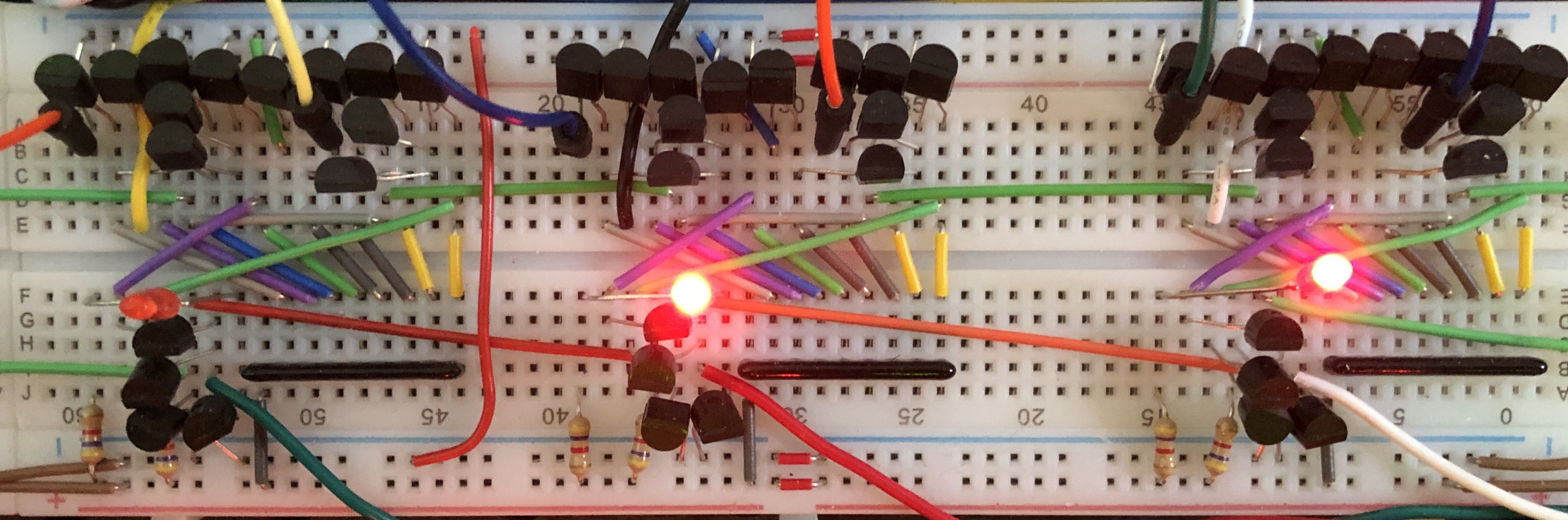
Here's a photo of the finished registers. CONSTANT is on top. Notice the blue LED in the INSTRUCTION register to indicate the state of the EN input.
![]()
The last CPU module is the Program Counter circuitry. Once that's done, I can start integrating everything and get to an actual working stand-alone CPU! Everything else (and there's a bunch!) will be bells and whistles.
-
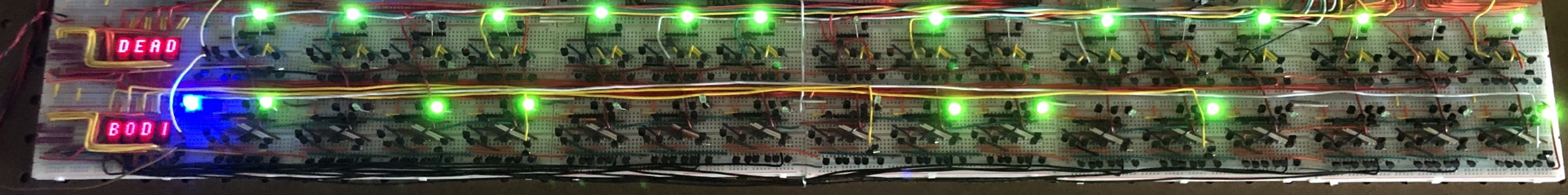
Making Memories
06/30/2019 at 15:55 • 0 comments![]()
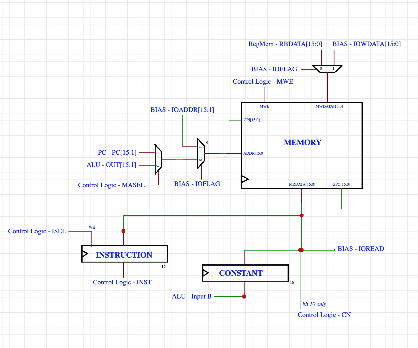
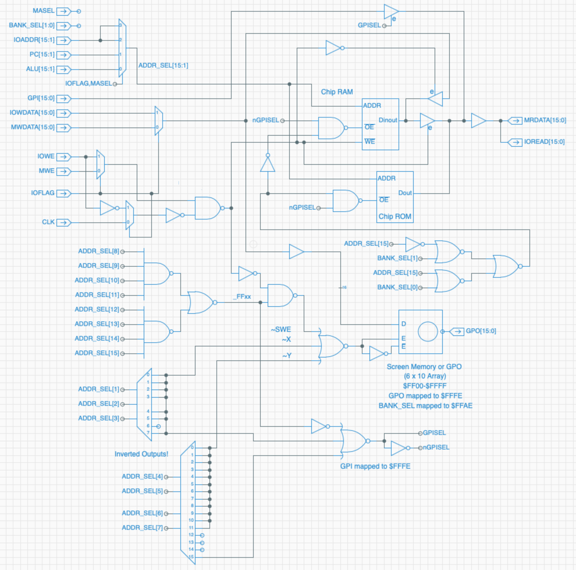
The Spikeputor memory module consists of two channels to address and read/write memory. One channel allows the CPU to access memory, and the other is used for DMA functions. The CPU can address memory from the Program Counter or from the ALU ouput, depending on the value of the MASEL (Memory Address SELect) signal. The DMA functions are performed by the BIAS card on the Apple II. Bringing the IOFLAG signal high pauses the CPU clock and redirects all memory access to BIAS. The memory is written to when either the MWE signal is high (set during the CPU STore command) or when the BIAS card sets IOW high. Memory data is available to be read by the CPU or BIAS as long as MWE (Memory Write Enable) is low. When high, MRDATA is undefined (high-Z). Memory data is stored in INSTRUCTION and CONSTANT registers as appropriate (discussed in the previous log entry). Additionally, bit 10 of the Memory data output is wired directly to the CN (Constant Needed) signal of the CPU Control Logic.
In addition to DMA, there are 16 bits of General Purpose Input and 16 bits of General Purpose Output. These are hard coded to memory location $FFFE and can be written to in order to set the GPO lines and read from in order to read the GPI lines regardless of the current settings of the RAM/ROM Bank Select (see below).
Memory storage is implemented in two ways. First, there are 32K words each of RAM and ROM, implemented by two each of 32K x 8 bit Static RAM (AS6C62256) and PROM (AT27C256R) chips. While RAM is always written to, whether RAM or ROM is read from depends on a bank-selection scheme, controlled by a two-bit specialty register, BANK_SEL. The value of BANK_SEL is set by writing the desired lower two bits to memory location $FFAE. RAM and ROM banks are accessed as shown in the table below:
BANK_SEL[0] = 0 BANK_SEL[0] = 1 BANK_SEL[1] = 0 RAM: $0000-$FFFF ROM: $0000-$7FFF
RAM: $8000-$FFFFBANK_SEL[1] = 1 (default)
RAM: $0000-$7FFF
ROM: $8000-$FFFFROM: $0000-$FFFF Second, there will eventually be 54 words of memory made via discrete transistors, resistors and LEDs, laid out to produce a 48 x 18 array of "screen memory" (this will be the last thing completed for the main Spikeputor boards). This memory will be "write-only," and will mirror chip RAM in the range $FF00-$FFFF.
The schematic of the memory modules is as follows:
![]()
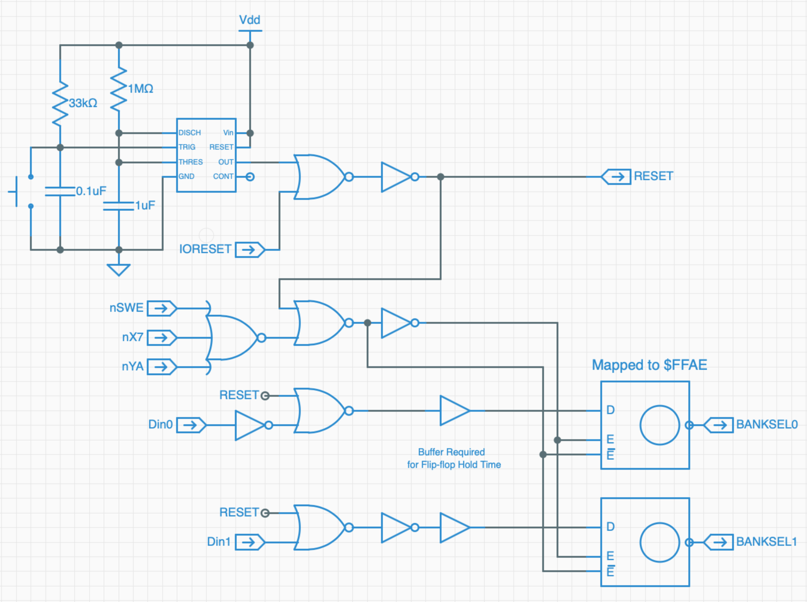
Finally, the power-up/reset logic is implemented via the following schematic. A RESET signal is simulated upon power-on and can be set manually via a debounced pushbutton or set via the BIAS card IORESET signal. RESET restores the BANK_SEL values to their defaults (0b10). The implementation of the simple memory elements for BANK_SEL was discussed in the "Building Blocks" section of the logs.
![]()
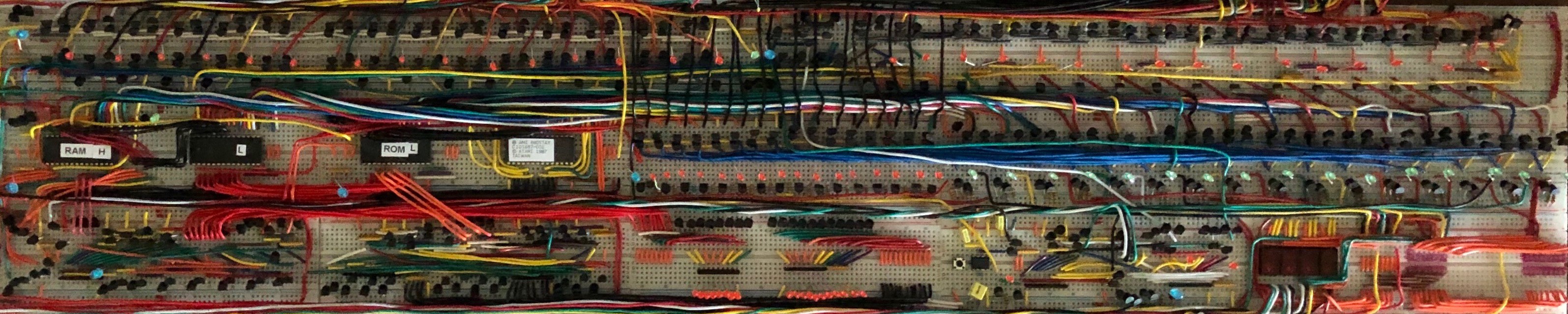
Here's a photo of the actual Memory Module, followed by a block diagram of everything that's going on.
![]()
![]()
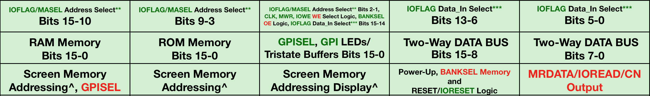
The top row handles the selection of address and data input based on the logic described above, implemented by a pair of MUX2's for address input and a single MUX2 for data input. The next row contains the actual RAM and ROM chips, the general purpose input logic and LED display, and the data bus. Finally, the third row contains the screen memory addressing logic (a 3 to 8 decoder and a 4 to 16 decoder, partially implemented) and display, the power-up/reset/bank_sel logic, and a numeric display and output ports for the memory data output.
Detailed photos of individual breadboards follow.
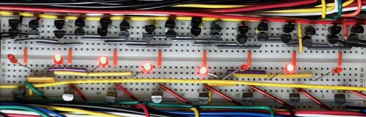
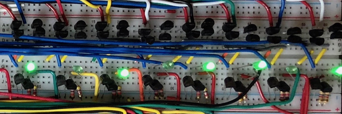
Six bits of the address select logic:
![]()
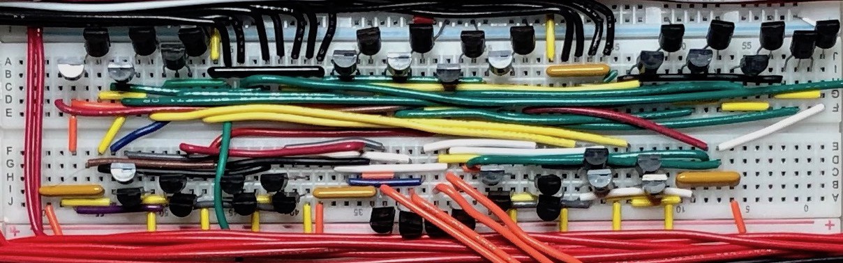
Eight bits of the data_in select logic:
![]()
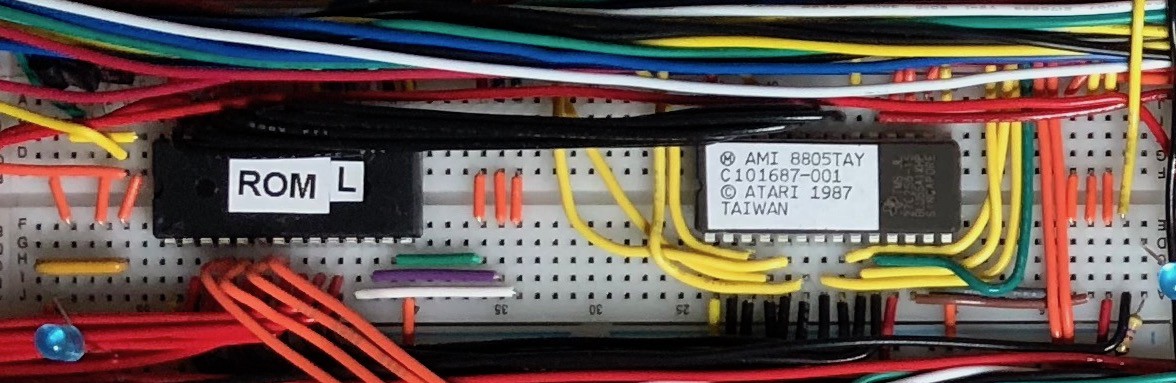
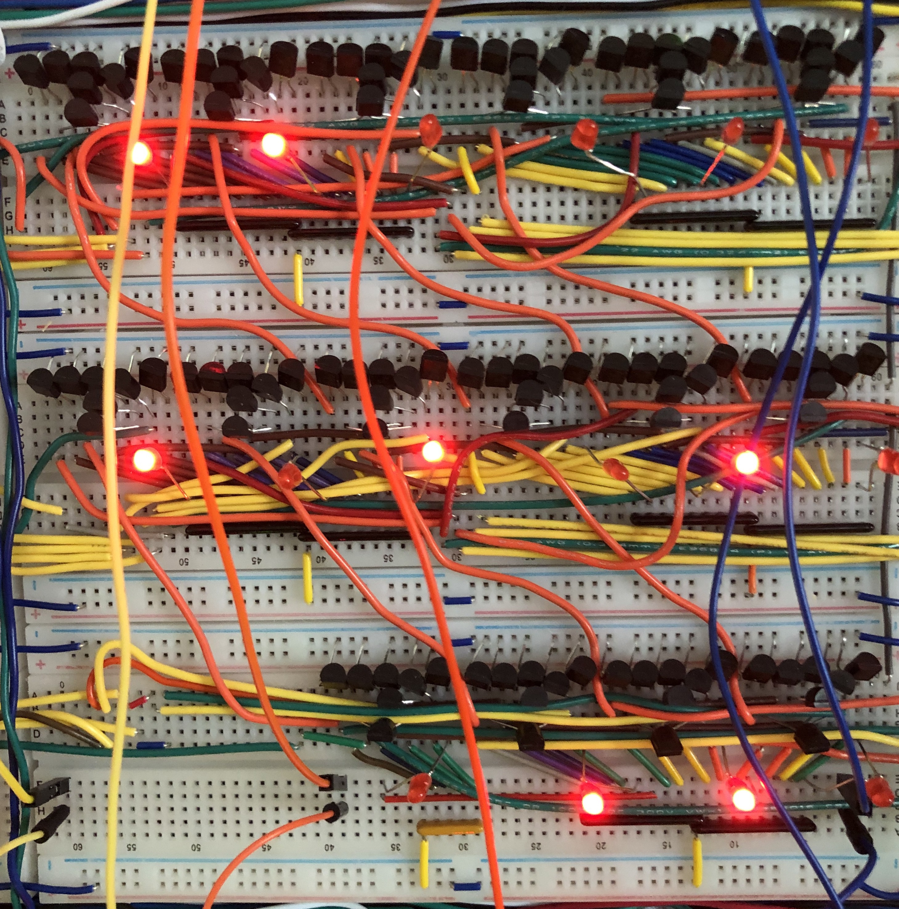
RAM Chip Memory:
![]()
ROM Chip Memory (including an old Atari ROM chip for testing):
![]()
Eight bits of the Data Bus:
![]()
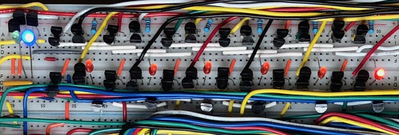
The 4 to 16 decoder for screen memory addressing, decoding the third nybble of the address. Only 11 lines are implemented since there are only nine rows of screen memory ($FF[0...9]x), plus one each to address BANK_SEL ($FF[A]E) and general purpose inputs and outputs ($FF[F]E).
![]()
The power-up/reset/bank_sel board:
![]()
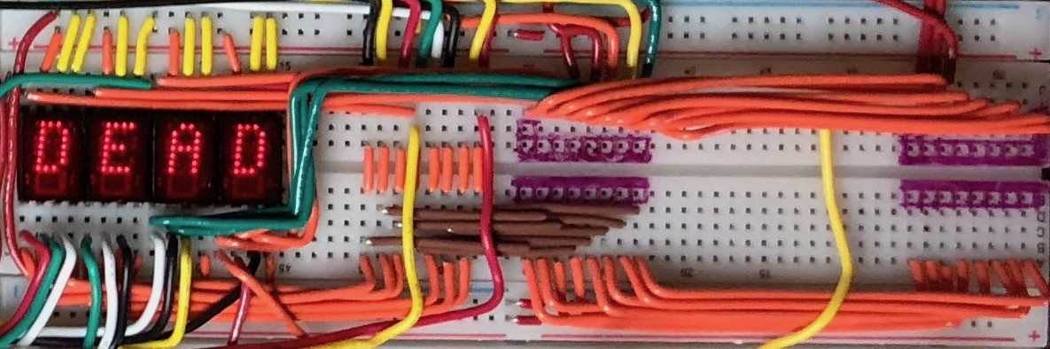
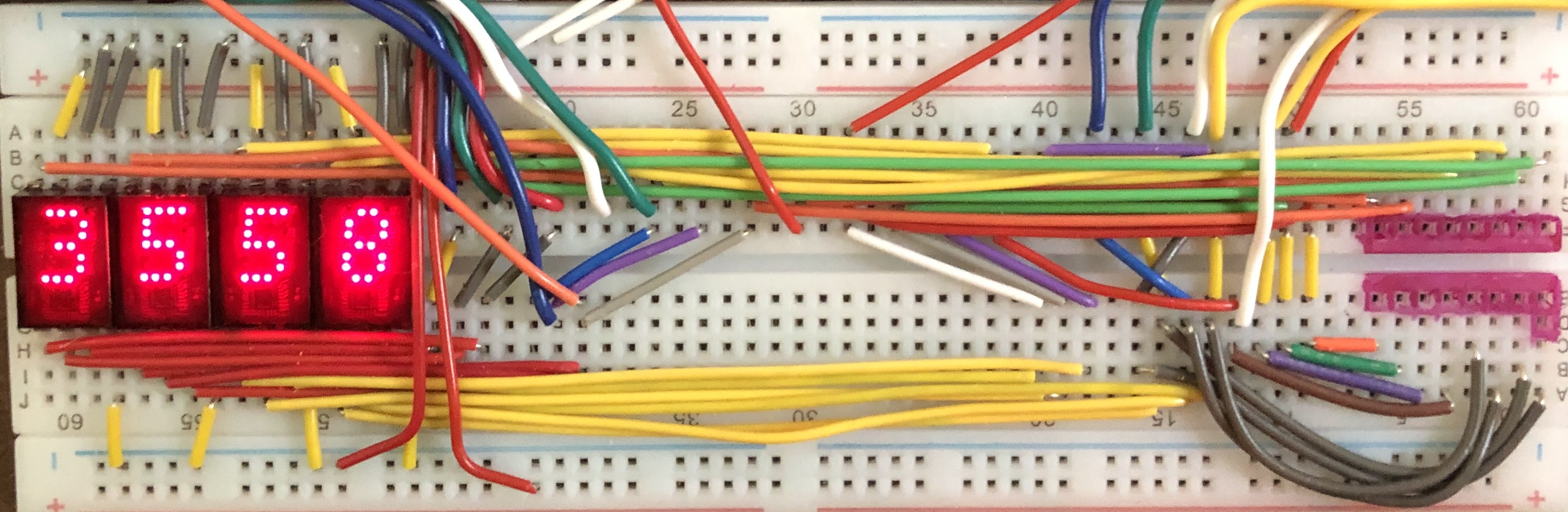
And finally, the Memory Data Output board, displaying one of my favorite hex numbers:
![]()
Next up: building the INSTRUCTION and CONSTANT registers, and then the Program Counter logic to complete the CPU!
-
Spikeputor ISA and Control Logic
05/02/2019 at 20:00 • 0 commentsEach Spikeputor instruction is one word (16 bits) long, with a subset of the instructions requiring a second 16-bit integer. Operations are divided into four groups: ALU Functions, Branching, Load, and Store.
ALU Functions
All ALU operations require two source operands, and one destination register. The two source operands are either two registers (Ra and Rb), or a register (Ra) and a 16-bit signed integer literal. The result of the ALU function is then stored in the destination register (Rc). Thus, ALU functions may either be one word or two words long, depending on the need for the 16-bit constant. Two-word instructions end in C.
ALU Instructions:
- Arithmetic
- ADD(Ra, Rb, Rc)
- SUB(Ra, Rb, Rc)
- ADDC(Ra, const, Rc)
- SUBC(Ra, const, Rc)
- Bitwise Logic
- AND(Ra, Rb, Rc)
- OR(Ra, Rb, Rc)
- XOR(Ra, Rb, Rc)
- ANDC(Ra, const, Rc)
- ORC(Ra, const, Rc)
- XORC(Ra, const, Rc)
- Bitwise Shift: The bottom four bits of the second operand represents the number of bits to shift. SRA is a right shift with sign extension.
- SHL(Ra, Rb, Rc)
- SHR(Ra, Rb, Rc)
- SRA(Ra, Rb, Rc)
- SHLC(Ra, const, Rc)
- SHRC(Ra, const, Rc)
- SRAC(Ra, const, Rc)
- Compare: Rc is set to 1 if the comparison is true, 0 if not. Comparisons are based on 2's complement signed integers except for CMPUL, which is an unsigned compare less than.
- CMPEQ(Ra, Rb, Rc)
- CMPLT(Ra, Rb, Rc)
- CMPLE(Ra, Rb, Rc)
- CMPUL(Ra, Rb, Rc)
- CMPEQC(Ra, constant, Rc)
- CMPLTC(Ra, constant, Rc)
- CMPLEC(Ra, constant, Rc)
- CMPULC(Ra, constant, Rc)
Branching
Conditional branch instructions test the value of register Ra. The branch is taken if Ra is zero (for BEQ) or not zero (for BNE). The second word of the instruction is used to specify a 16-bit signed Program Counter offset. Before the branch, register Rc is loaded with the next calculated Program Counter value so it may be used as a return vector. If the branch will be followed, the target branch address is calculated by adding the given offset to that new PC value.
For immediate branching, there are two options: JMPC calculates the target branch address by adding the value of Ra to the given 16-bit signed literal. JMP simply takes the target branch address from the value of register Ra. As with the conditional branches, Rc is set to the address of the subsequent instruction. Branch instructions are two words long except for JMP. Also, if Ra is register 6, the JMP(R6, Rc) instruction will clear the IRQ flag, indicating the end of interrupt processing.
Branching Instructions:
- BEQ(Ra, PC offset, Rc)
- BNE(Ra, PC offset, Rc)
- JMPC(Ra, mem offset, Rc)
- JMP(Ra, Rc)
Load
There are two load instructions to move values from memory into registers. Both instructions use two words, the second of which is used as a signed memory offset. For the LD instruction, the target memory address is calculated by adding the value of register Ra to the given offset . The LDR (LoaD Relative) instruction adds the offset to the memory address of the subsequent instruction. In both cases, the data in the calculated memory address is stored in register Rc.
Load Instructions:
- LD(Ra, mem offset, Rc)
- LDR(PC offset, Rc)
Store
The only way to write to main memory is through the two-word Store instruction. The value of register Rc is stored in the memory address calculated by adding the value of register Ra to the value of the second word.
Store Instruction: ST(Rc, Ra, mem offset)
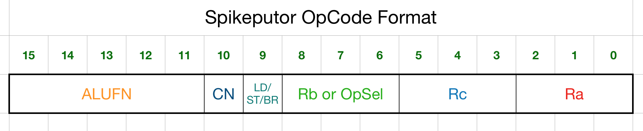
The format of the opcodes are as follows:
![]()
The top five bits of the opcode are simply the ALU function (described in the ALU log entry) and are passed directly to the ALU. Bit 10 (Constant Needed) indicates whether or not the opcode is made up of a one word or two words. Bit 9 differentiates between ALU functions and the other Spikeputor operations (Load/Store/Branch). If bit 9 is clear, the next three bits (bits 8-6) encode the register address of the second operand, Rb. The Rb bits are ignored for ALU functions that use the second word as a constant. If bit 9 is set, the instruction is determined from bits 8-6 as follows:
- 0b000: JMP
- 0b001: <undefined>
- 0b010: LD
- 0b011: ST
- 0b100: BEQ
- 0b101: BNE
- 0b110: LDR
- 0b111: <undefined>
Bits 5-3 encode the register address of Rc, and bits 2-0 encode the register address of Ra.
Control Logic
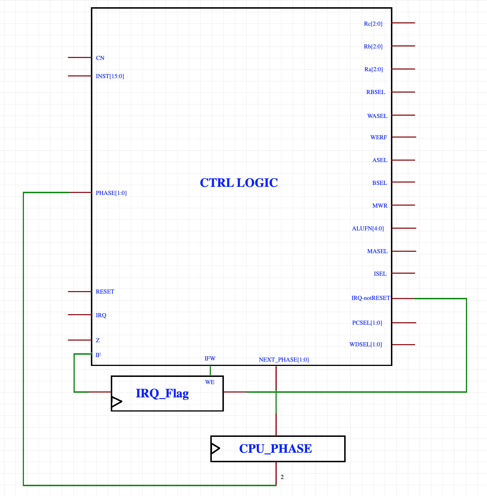
The control logic of the Spikeputor translates the opcodes plus a few flags into a series of control signals. The signals select the appropriate CPU phase, keep track of the IRQ status, and set up the appropriate logic paths in order to execute the current instruction. Signals, flags and control logic are described in detail below.
![]()
Each instruction takes two or three clock cycles (CPU phases) to perform. The PHASE signal keeps track of these steps. Upon reset and power-up, PHASE is set to 0.
Control Logic Inputs are as follows:
- The input CN (Constant Needed) is directly wired to bit 10 of the main memory data output.
- INST is the 16-bit output of the INSTRUCTION Register.
- RESET is the hardware reset line.
- IRQ is the hardware interrupt line.
- Z is the output of Zero Detect logic applied to the Register Memory Channel A output.
- IF is the output of the IRQ_Flag status bit.
When PHASE is 0 and there is no RESET or IRQ signal, an opcode is read from the memory address pointed to by the Program Counter (PC) register and placed on the input of the INSTRUCTION register, to be stored on the next clock pulse. CN is immediately used to determine if a second word needs to be read for the instruction.
If CN is 0, NEXT_PHASE is set directly to 2 and the PC will not be incremented. Otherwise, NEXT_PHASE is set to 1 and the PC is incremented. On the next clock cycle, PHASE will be 1. Memory at the new PC address is read into the CONSTANT register and the INSTRUCTION register is not updated (It will still contain the instruction opcode from Phase 0). NEXT_PHASE is set to 2 and the PC is not incremented.
On the next clock cycle, PHASE will be 2. This is the phase where the instruction is executed. The ALU function, register addresses, and all other logic pathways will be set based on the Control Logic Inputs. The PC will be updated (either incremented or updated with the new "jump to" address), and NEXT_PHASE is set back to 0, starting the next instruction cycle.
If the RESET signal goes high at any time, PHASE is reset to zero, the IRQ flag is cleared, all memory write and register write signals are cleared, and the NEXT_PC register is set to the Reset vector via the PCSEL signal (described below).
If the IRQ signal goes high, RESET is low, the IRQ_FLAG (IF) status bit is currently clear, and PHASE is zero, the IFW (the IRQ Flag Write) signal is set so that on the next clock pulse, the IRQ_FLAG will be set. R6 is set to be written to with the current PC address, and NEXT_PC is set to the Interrupt vector via the PCSEL signal. The IRQ signal is ignored if IF is already set, PHASE is not zero, or RESET is high. Systems invoking the Spikeputor IRQ signal should only set it during CPU phase 0. The BIAS card will capture this information by looking at the ISEL signal, which is high only during that phase.
The remaining signals have the following meanings and are mainly used to set up the logic pathways for each instruction. Each signal is one bit unless otherwise noted. See the Spikeputor Main Schematic for the high level view:
- Ra, Rb, Rc (3 bits each) are the three register address inputs to the Register Memory module. They are directly copied from the appropriate bit fields of the opcode as described above. Ra specifies which register address is output on Register Channel A. Rb and Rc are used as described below.
- RBSEL selects whether the Rb or Rc operand from the opcode specifies the register address to output on Register Channel B (0: use Rb, 1: use Rc).
- If WERF is high, the WData Input is written to the selected input register on the next clock cycle. If WERF is low, the previous value of that register will be maintained. The input register is determined by Rc and the value of WASEL.
- WASEL selects whether the input register is set to Rc or if the exception register (R6) will be written to (0: use Rc, 1: use R6).
- ALUFN (5 bits) is sent directly to the ALU to select ALU function and output channel. These five bits are directly copied from the opcode as described above.
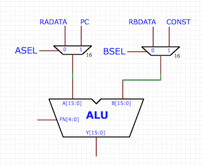
- ASEL selects whether ALU Input Channel A will come from Register Memory Output Channel A or from INC_PC, the incremented value of the program counter. (0: Register Memory, 1: Program Counter).
- BSEL selects whether ALU Input Channel B will come from Register Memory Output Channel B or from the CONSTANT register (0: Register Memory, 1: CONSTANT).
- MWR selects whether or not to enable writing to main memory (0: do not write, 1: write).
- MASEL selects whether the main memory address is selected from PC (the Program Counter) or from the ALU Output. (0: Program Counter, 1: ALU).
- ISEL selects whether the INSTRUCTION register will be updated from Memory Data Output on the next clock cycle or will maintain its current value (0: do not update, 1: update)
- IRQnotRESET is the logical AND of IRQ and NOT(RESET), meaning that it will be high if IRQ is high and RESET is low, and low in all other circumstances. It is used to update the IRQ_FLAG and select between the RESET vector and IRQ vector in the Program Counter module.
- PCSEL (2 bits) selects how the value of PC is calculated for each clock cycle:
- 0: Maintain the same value.
- 1: Increment the PC (PC = PC + 2).
- 2: Use IRQnotRESET to produce the RESET vector ($FD00) or the IRQ vector ($FE00).
- 3: Use the JT (Jump To) value, provided by the ALU Output.
- WDSEL (2 bits) selects the source of the Register WData Input:
- 0: Use the PC_INC output.
- 1: Use the ALU output.
- 2: Use the Memory Data output.
- 3: Use the PC output.
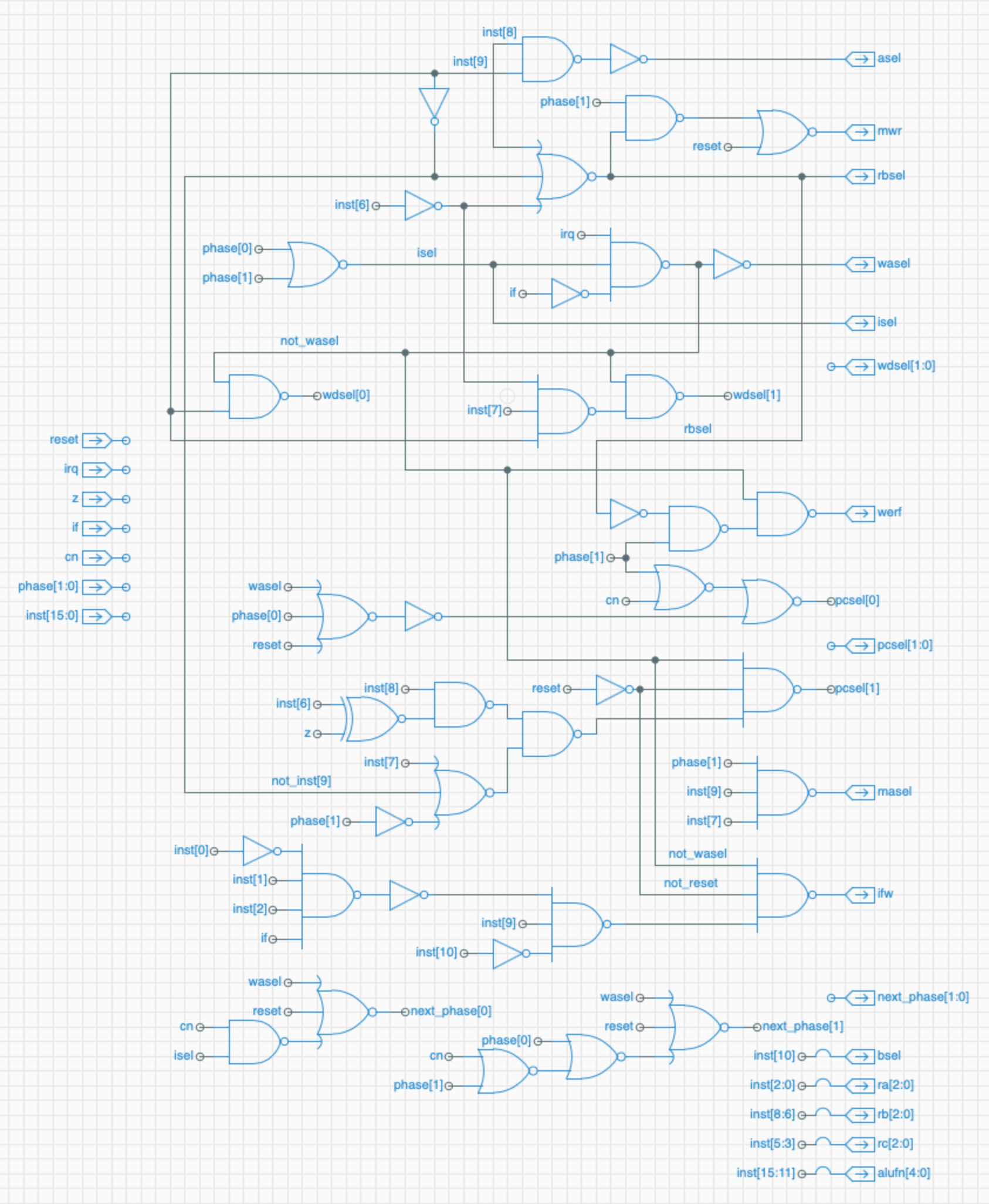
The schematic for the Control Logic is shown below. It simply translates the logic listed above to circuitry. Not shown are the circuits for the flip-flops that store the PHASE and IF status bits. They are similar to the Register Memory Flip-Flops described in an earlier log entry.
![]()
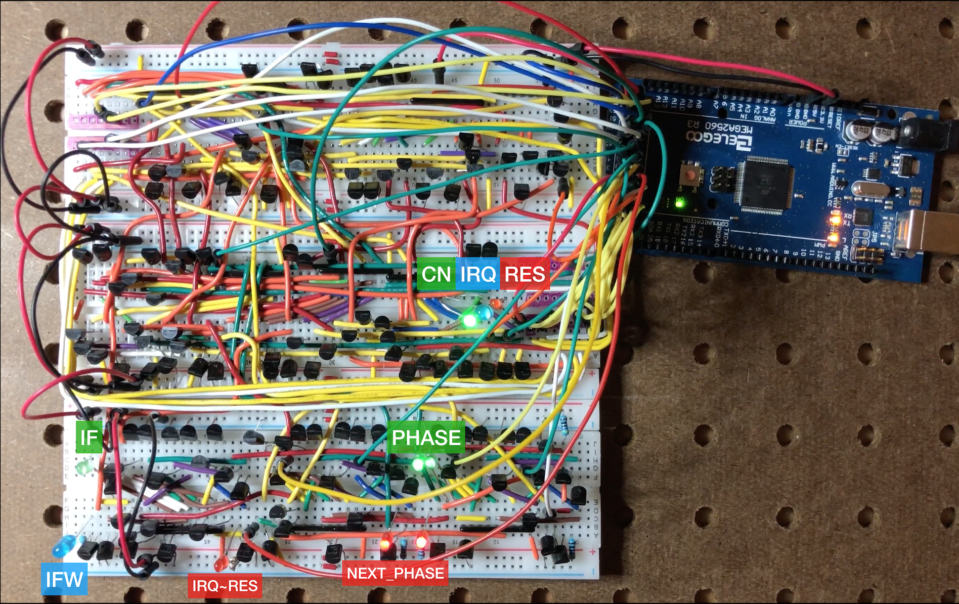
To test the implementation, I programmed a Mega2560 to output all possible combinations of inputs, captured all of the outputs, and then compared the output values with calculated values. Here's a photo of the completed board, hooked up to the Mega2650:
![]()
In the following video, you can see the rapidly changing PHASE and NEXT_PHASE signals, as well as a few flashes of IRQ, IFW and IF being stored and cleared. I also show how the Mega sends the Control Logic outputs to the computer for analysis. After a few quick wiring fixes, the boards work as specified. Not too bad for 130 transistors!
- Arithmetic
-
It's About Time!
04/27/2019 at 22:56 • 0 commentsUntil now, I've been generating clock signals via an Arduino. With the Register Memory and ALU boards complete, and work beginning on Control Logic, it was time to think about building a clock for the Spikeputor. Like many other homebrew computers, I wanted the clock rate to be variable based on user control of some kind of knob or slider. I also wanted the ability to switch to a mode where the user can control the clock pulses on a step-by-step basis for a fine-grained look at the CPU in action.
Because everyone loves a 555, I decided that it would be an appropriate timekeeper for the Spikeputor. I considered creating a discrete version (see this great kit, for example), but since space on the pegboards was filling up fast, I decided to start with ICs, and then go discrete later on if space is available.
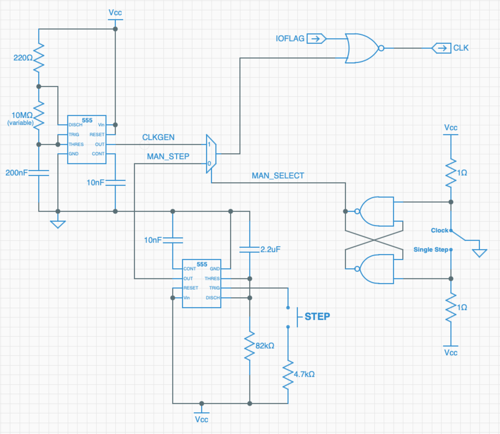
Here's the schematic for the clock circuit:
![]()
I'm actually using two 555's - one to generate the variable-rate clock signal, and another to generate a clean 200 ms debounced pulse for the manual step pushbutton. Using a 10 MΩ variable resistor and a 200 nF capacitor, clock rates between 0.35 and about 17,000 Hz are possible. I might want a little more dynamic range, so I'm considering switching to a control knob where I can substitute a larger range of resistors, but for now, the 10 MΩ slider will do.
The 555 clock signal and the single step pulses go into a 2-channel MUX, the output of which is controlled by a Clock/Step Select switch, itself debounced via an SR latch. Finally, one final gate allows for setting IOFLAG high to stop the clock so the DMA I/O can occur.
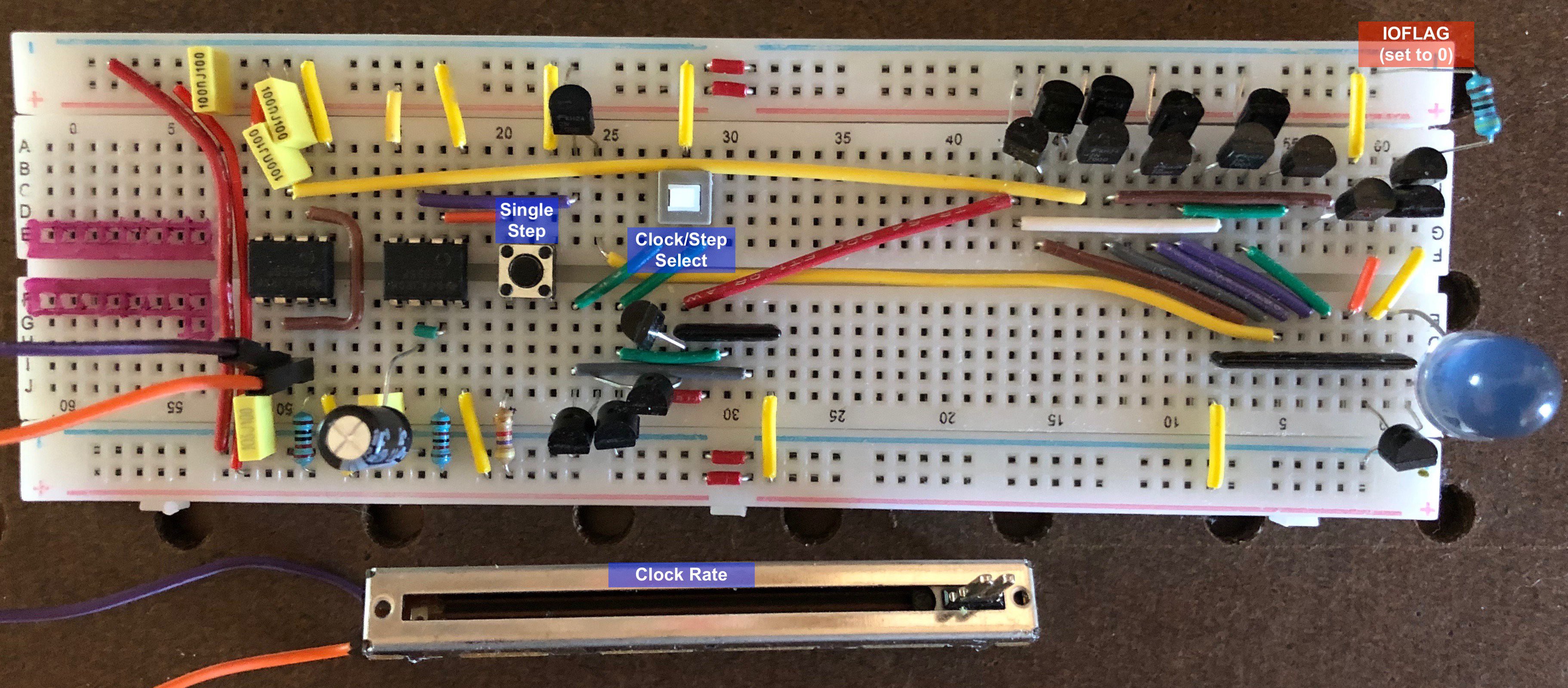
Here's how it all fits together on a board:
![]()
IOFLAG is hard-wired to 0 right now, but that will eventually connect up to the BIAS board of the Apple II for I/O.
And here's a little demo of the board in action. We start in clock mode, adjust the rate, then switch over to single-step mode, step a bit, then switch back to the clock. This board drives the proto-Spikeputor perfectly!
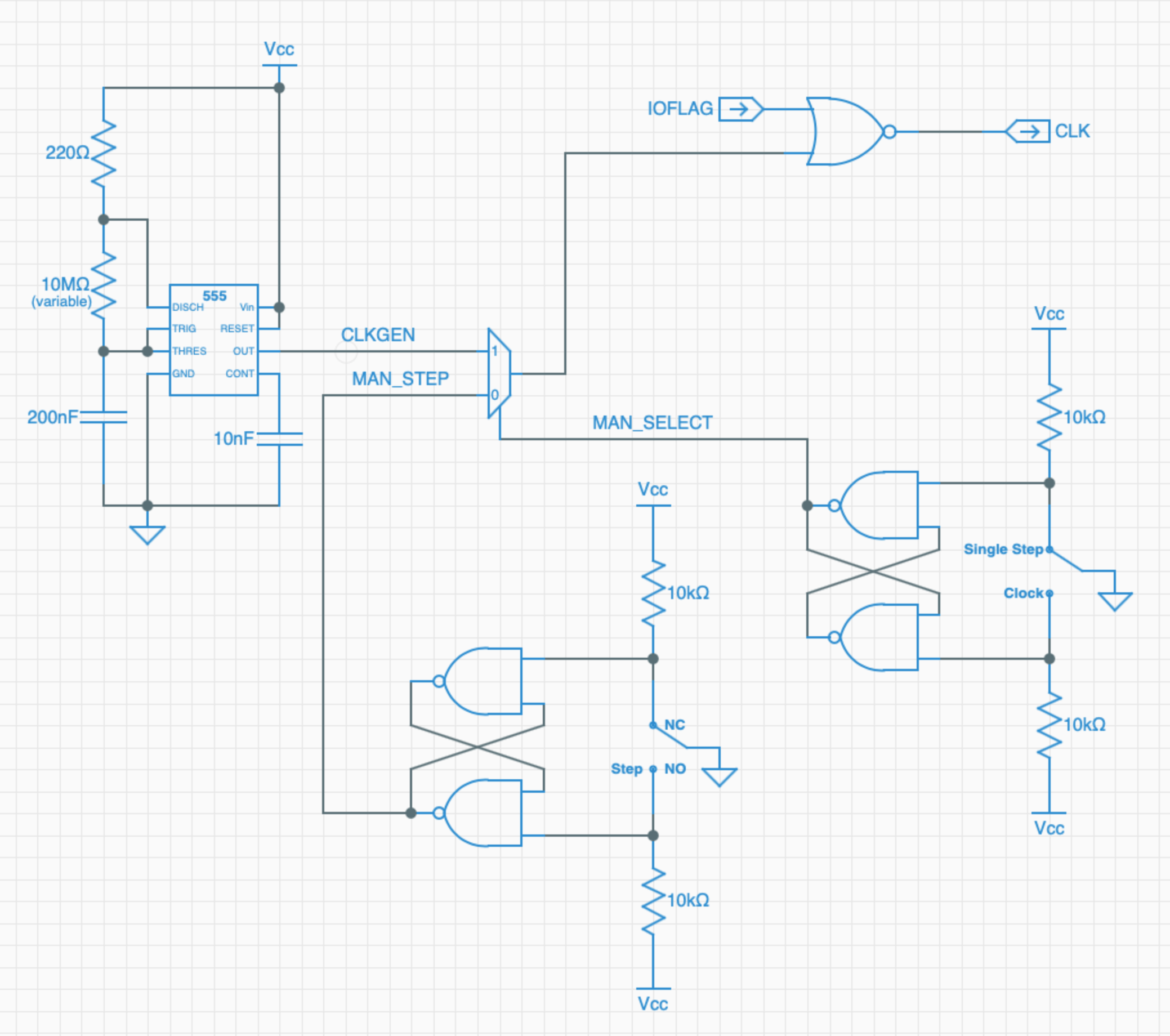
UPDATE: I decided to eschew one of the 555 chips in anticipation of eventually replacing the single remaining 555 with discrete components. Instead, I used a DPST momentary pushbutton switch for the single step pulse, debounced via another SR Latch as shown here:
![]()
-
I'm a Big Fan of Sharp Clock Signals
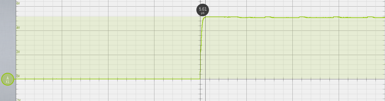
04/06/2019 at 18:03 • 0 commentsAs work on the Spikeputor continues, I wanted to check out the shape of the clock pulses, now that a single signal feeds into 112 inputs (7 registers * 16 bits per register). In the entire design, there will be upwards of 165 clock inputs. The result of such a high fan-out number was not entirely unexpected:
![]()
At 37 µS for full rise, that starts rivaling the top speed I want to be able to run the processor (~40 µS, preferably faster if I can speed up the ALU). All of those tiny capacitances of each of the input transistors are starting to add up, slowing down the rise time! Luckily, there's a simple solution to this expected problem: build a clock tree. I inserted a buffer (two transistors) in front of every group of 16-bit inputs, and now the rise time is seven times faster. Math and physics works! Yay!
![]()
None of this is rocket science, but it's a very helpful and educational illustration of these principles. Onward!
-
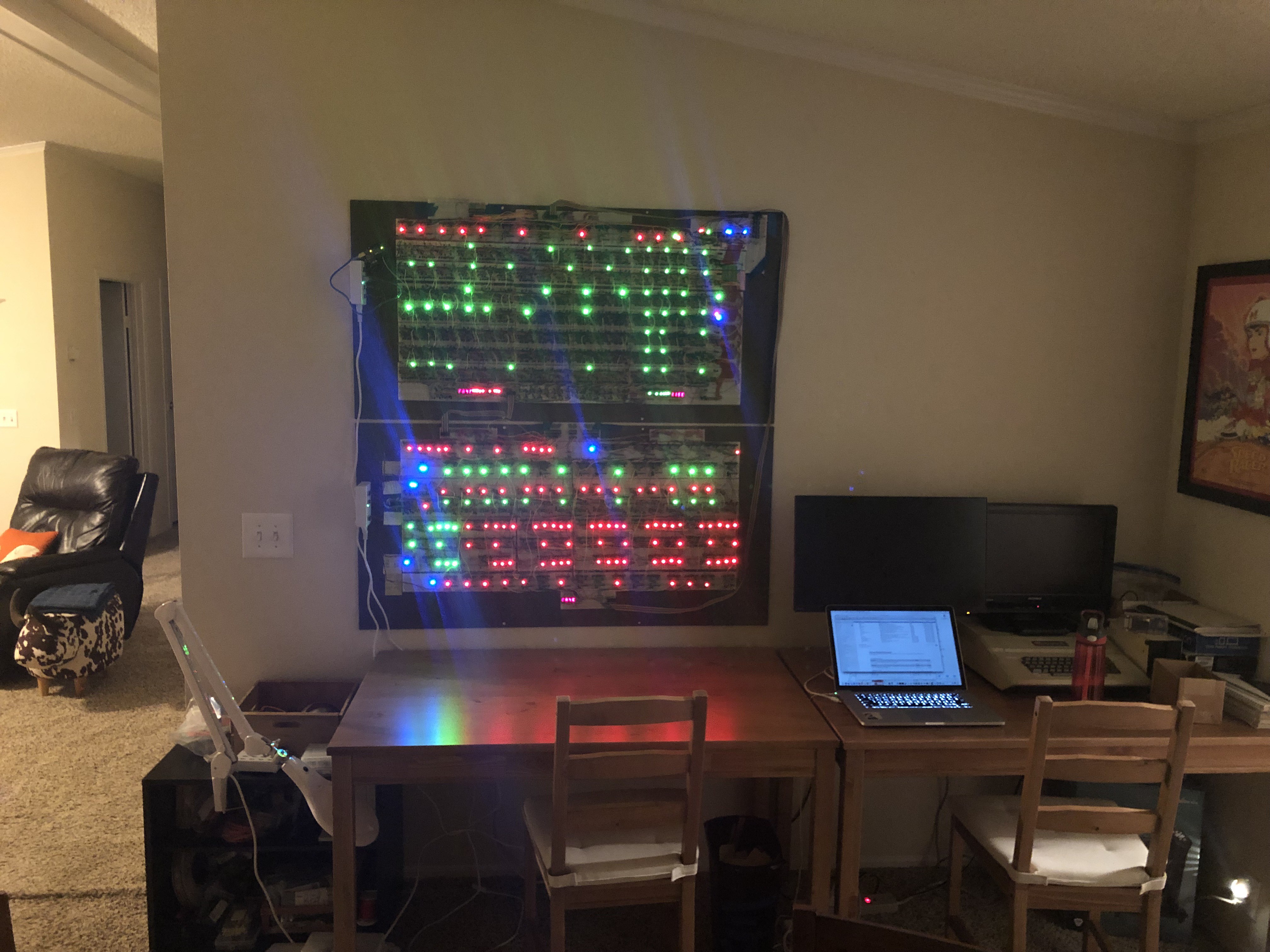
ALU and RegMem Completed - Demo Time!
03/02/2019 at 22:15 • 5 commentsTwo of the four major pegboards of the Spikeputor are now complete and have been mounted. They come down pretty easily in case repairs or modifications need to be made that can't be performed right on the wall.
![]()
Now that we have seven functioning registers and an ALU, we can put it through its paces by simulating the rest of the CPU. Wiring together the components along with an Arduino, the nascent CPU can be "programmed" by simply setting up the correct input signals after every rising clock pulse (also provided by the Arduino).
![]()
Since there is no RAM yet, the only storage is in the registers. Nevertheless, you can easily set up the Arduino to do something like this:
- Place the correct values in each of the registers:
- Select the register with Ra and Rc to output to Channel A and to allow the input to overwrite it (Rb is ignored)
- Turn Write Enable on
- Output the correct bit pattern to the CONSTANT input.
- Set ASEL to 0 (input from Register Channel A goes to ALU A)
- Set BSEL to 1 (input from CONSTANT goes to ALU B)
- Set the ALU to the ADDC function to add Input A to Input B.
- Rotate Left each of the registers:
- Select the register with Ra and Rc to output to Channel A and to allow the input to overwrite it (Rb is ignored)
- Turn Write Enable on
- Output 0x0001 to the CONSTANT input.
- Set ASEL to 0 (input from Register Channel A goes to ALU A)
- Set BSEL to 1 (input from CONSTANT goes to ALU B)
- Set the ALU to the Rotate Left function to rotate Input A by Input B bits.
- After doing this for all seven registers, pause briefly and loop back to another rotate cycle
And voilá! Ghost In The Machine!
You can also set up a similar type of loop, except instead of shifting bits, you can add a constant. This video starts with adding 1 by setting the ALU A Input DIP switch to 0x0001, outputting the selected register to Channel B with write-back, and cycling for a number of clock cycles before moving on to the next register. It shows the whole CPU, then focuses on the ALU output, and then Register Output Channel B. The DIP switch is then changed to 0x0010 to increment the second digit (by adding 16), leaving the first digit intact.
Finally, for something a bit more advanced, we can manipulate the control signals to simulate a program to calculate the first 24 Fibonacci numbers (all of them that can fit in 16 bits). After each number, the control signals are set to place the step number on RegMem Output Channel A and the corresponding Fibonacci number on RegMem Output Channel B, then pause before calculating the next one. The "program" uses four registers:
- R0 = N
- R 1 = Fib(N-2)
- R2 = Fib(N-1)
- R3 = Fib(N)
(Video in the dark for dramatic effect!)
- Place the correct values in each of the registers:
-
Adding an Unsigned Compare Function to Enable Wide Math
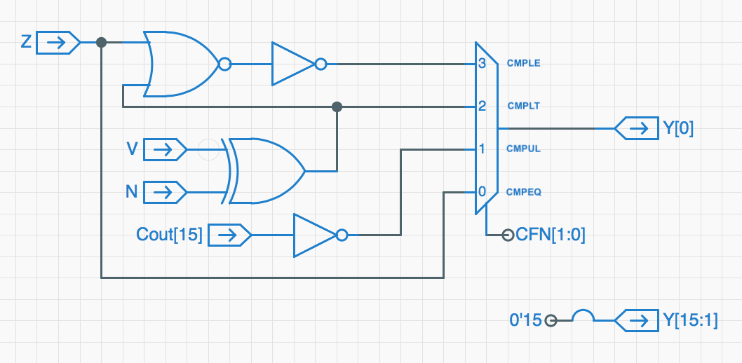
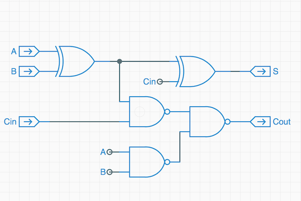
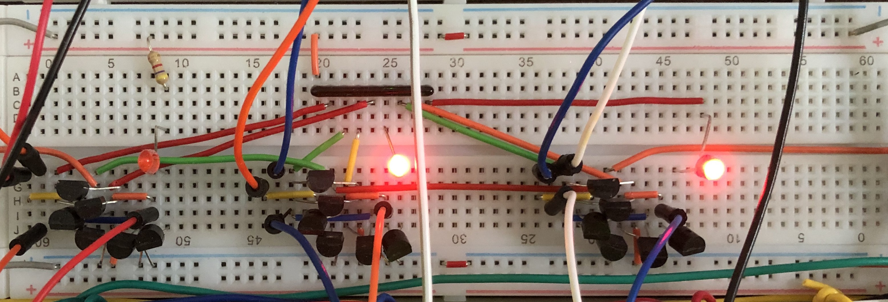
02/18/2019 at 21:49 • 0 commentsAs currently designed, the Spiekputor's ALU Compare functions worked with signed integers only. For whatever reason, the "Beta" processor from MITx, upon which the Spikeputor CPU was based, only included signed compares (so, for example, the number 0xC000 would be reported as less than 0x7000 because 0xC000 represents the signed integer -16384, rather than the unsigned integer 49152). This presents a problem if one desires to do math on numbers of a higher bit depth than the bit depth of the CPU registers and the ALU. To add two 32-bit numbers with a 16-bit ALU, for example, you need a way to calculate the carry after summing the lower 16 bits of the 32-bit numbers, then add that carry to the sum of the higher 16 bits. Calculating the carry can be done a variety of ways in code, but it comes directly by checking if the low order sum is less than either of the addends. Thus, an Unsigned Compare Less Than function would be a great addition to the ALU commands. Luckily, it was fairly easy to add the new compare function by expanding the Compare module, which simply subtracts one operand from the other and reports a result based on logic with (Z)zero, (N)egative, and o(V)erflow flags. Adding one more compare function (CMPUL for CoMPare Unsigned Less-than), and bringing in the Carry Out from the Bit 15 adder, as shown below, does the trick.
Previous Compare Module:
![]()
New Compare Module:
![]()
This change adds just four transistors to the circuit (converting a MUX3 to a MUX4 and inverting Cout[15]), and now, the Spikeputor will be able to easily do math on numbers arbitrarily larger than 16 bits. A very small price to pay, indeed!
-
Caught Up To Real Time! Current Status
01/29/2019 at 17:42 • 0 commentsSince I started this Hackaday project after I had completed a portion of the actual Spikeputor, I've spent the last few months catching Hackaday up to the current state. As of now, the "history" is complete in the logs and it'll be progress in real time from here on out!
Here is a summary of the current state of Spikeputor project. Additional details will be addressed in separate Project Logs.
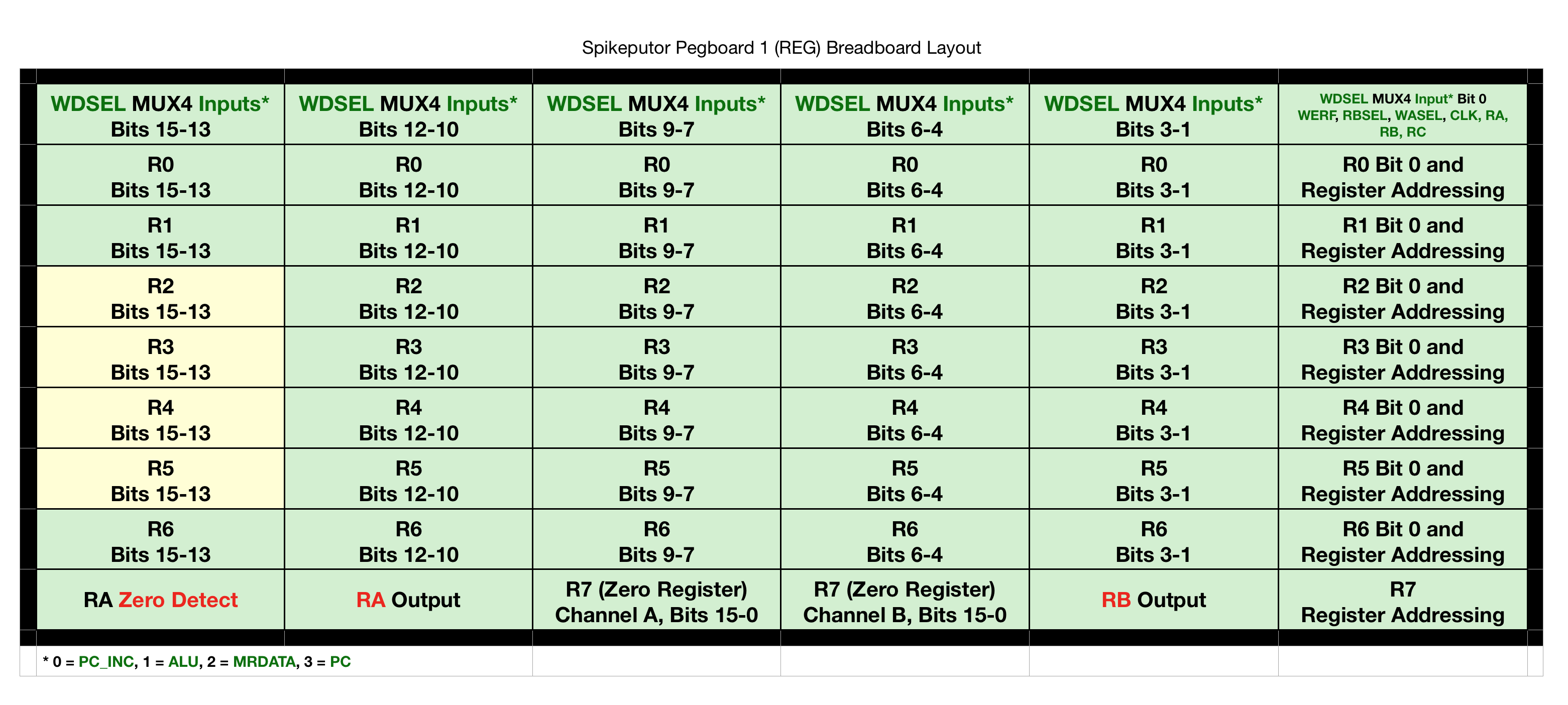
Pegboard 1 - Register Memory: All but three bits of four registers are completely assembled.
![]()
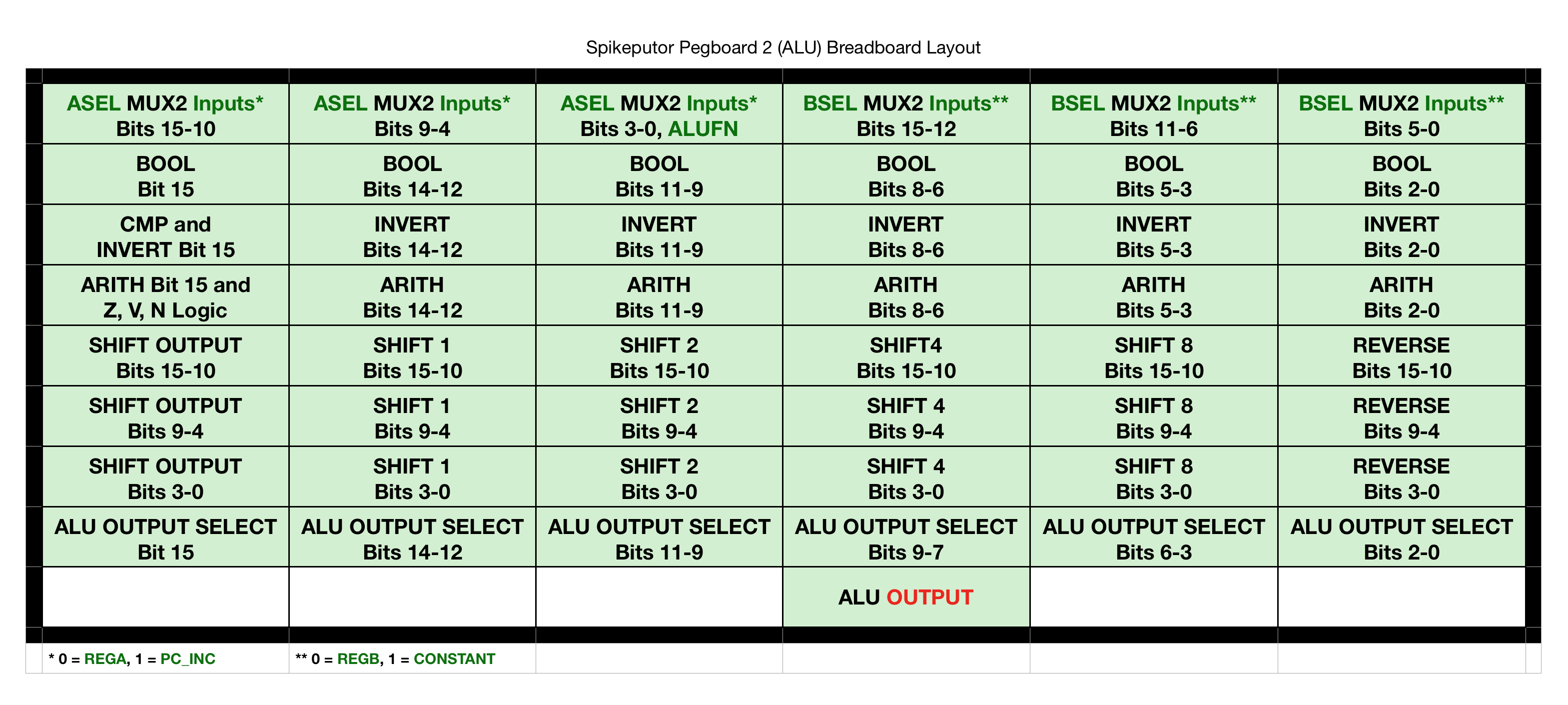
Pegboard 2 - ALU: Entirely assembled.
![]()
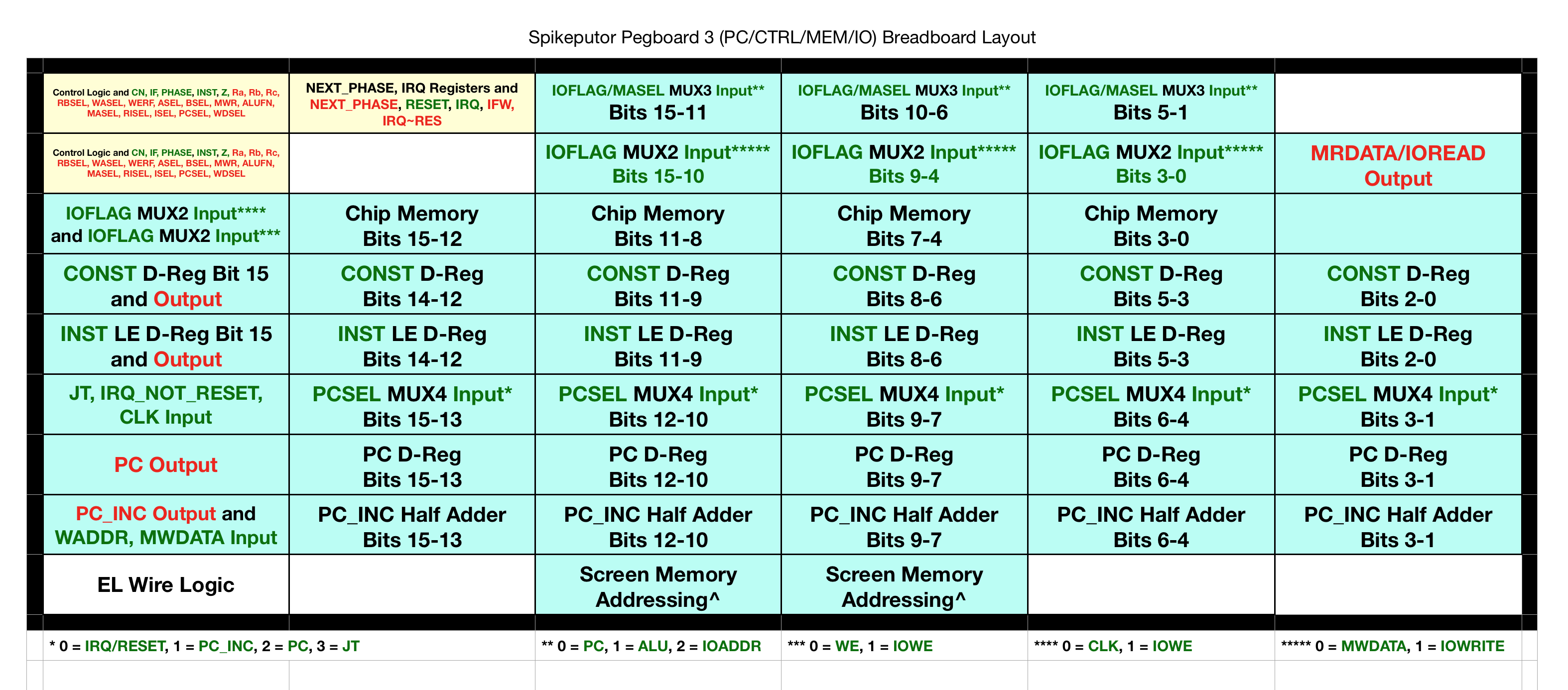
Pegboard 3 - Control Logic, CONSTANT and INSTRUCTION registers, Program Counter, Memory Addressing, Main Memory, EL Wire Logic and System Clock: most circuits are designed, but the breadboard layouts are not yet completed (blue cells). Control Logic layout is designed and ready to be assembled.
![]()
Pegboard 4 - Screen Memory: Circuit design and breadboard layout completed and ready to be assembled, but this will only happen after Pegboard 3 is complete and the CPU is otherwise functional.
![]()
BIAS (Board to Interface Apple to Spikeputor) Card: Circuit designed and assembly in progress.
In addition, I have written a custom Spikeputor simulator to confirm that the overall design and especially the control logic should work as planned.
I have also written an assembler for the Spikeputor instruction set.
-
Designing and Building the ALU
01/29/2019 at 15:35 • 0 comments![]()
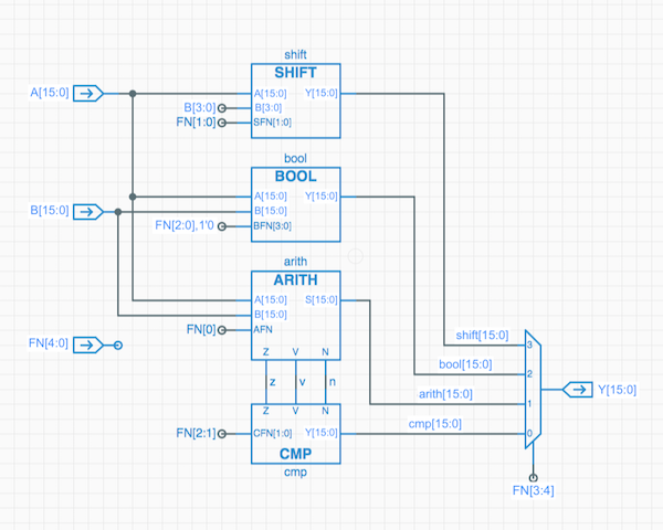
The ALU is the second major module of the Spikeputor, and, including the two input MUX2's, fits neatly on a single pegboard. The design of the ALU again mimics the design of the MITx "Beta" microprocessor. The major differences are the 16 bit (vs. 32 bit for the "Beta") data widths and the fact that, since the opcode width is reduced, the ALU FN input is five bits wide (vs. six). As a result, I needed to take a shortcut with the Boolean module function select (described below). The high-level ALU schematic simply routes the inputs A and B through the four ALU modules and routes the desired function through the function-select MUX4 to the output:
![]()
Here's six bits of one of the input MUX2's, placed at the top of the pegboard. The two MUX2's will select between the Register A input and the next PC value (ASEL signal) and between the Register B input and the CONSTANT value (BSEL signal):
![]()
The ARITH module performs addition and subtraction. The heart of the design is a 16 bit ripple carry adder. If AFN (bit 0 of the ALU FN) is 1, the B input is inverted and the initial full adder carry is set to 1. This produces the 2's complement form of the input (B XOR 0xFFFF + 1), and thus, outputs the difference instead of the sum of A and B. There is also logic to determine whether the result is (N)egative, (Z)ero, or caused an o(V)erflow. These flags are used as inputs to the CMP module.
![]()
The full adder circuit is standard:
![]()
The physical layout of the ARITH function places the B Input inverters directly above the full adder circuitry, keeping all of the bits aligned. This creates some empty space on the inverter breadboards, but greatly simplified the wiring between rows.
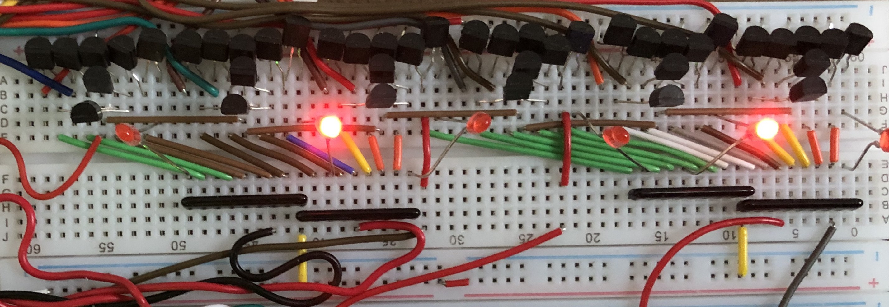
Three bits of inverter:
![]()
And three bits of full adder:
![]()
The breadboards used to add and invert the high order bit have extra space on them, and so they conveniently accommodated the N, Z, and V flag logic and the entirety of the CMP module. The CMP circuit just takes A - B from the ARITH modules and looks at those three flags to determine the single bit output based on the value of CFN (bits 1 and 2 of the ALU FN):
![]()
The BOOL module provides bitwise logic operations between the two inputs. Each bit of the module simply combines the A and B inputs to create a two bit select signal for a MUX4. The four inputs of the MUX then correspond to the truth table for each pair and A and B bits. In the original "Beta" design, each of these four values was directly taken from the ALU FN, allowing for instructions that can create any two-input logic function. Because I only had five bits to use for the entire ALUFN, and two of those ware used to select which module to output, I was forced to make do with the remaining three bits for the BFN input. Luckily, all of the major logic functions I wanted to implement (AND, OR, XOR, and A Identity) can be produced with three bits, hard-wiring channel 0 of the MUX4 to 0.
![]()
To produce an AND function, BFN is 0b100. OR is 0b111, XOR is 0b011, and the A Identity function is 0b101.
Three bits of BOOL:
![]()
The SHIFT module is considerably more complicated. It takes the lower four bits of Input B to determine how many bits to shift Input A. Depending on the SFN inputs, the bits are shifted to the left or right, and with or without sign-extending bit 15. The sub-module is implemented with a cascade of six MUX2's. Four MUX2's shift the number 1, 2, 4, or 8 bits to the left or allow it to simply pass through, depending on the value of Input B. The remaining two MUX2's reverse the bit order of Input A and reverse it back after the shift operations in order to procedure right-shifted results:
![]()
The physical layout of the SHIFT module breaks with the usual one row per word design, instead placing each of the MUX2's in a single column that is three rows tall. Here's one column of the SHIFT module, which corresponds to all 16 bits of the SHIFT4 MUX2 in the schematic:
![]()
The output of each module is directed to a MUX4 to select the ALU output. These boards are physically below all of the other ALU modules:
![]()
Finally, at the very bottom of the pegboard is the ALU Output board, which features a numeric display and an area for a 16-pin ribbon cable to direct the ALU Output to the rest of the CPU:
![]()
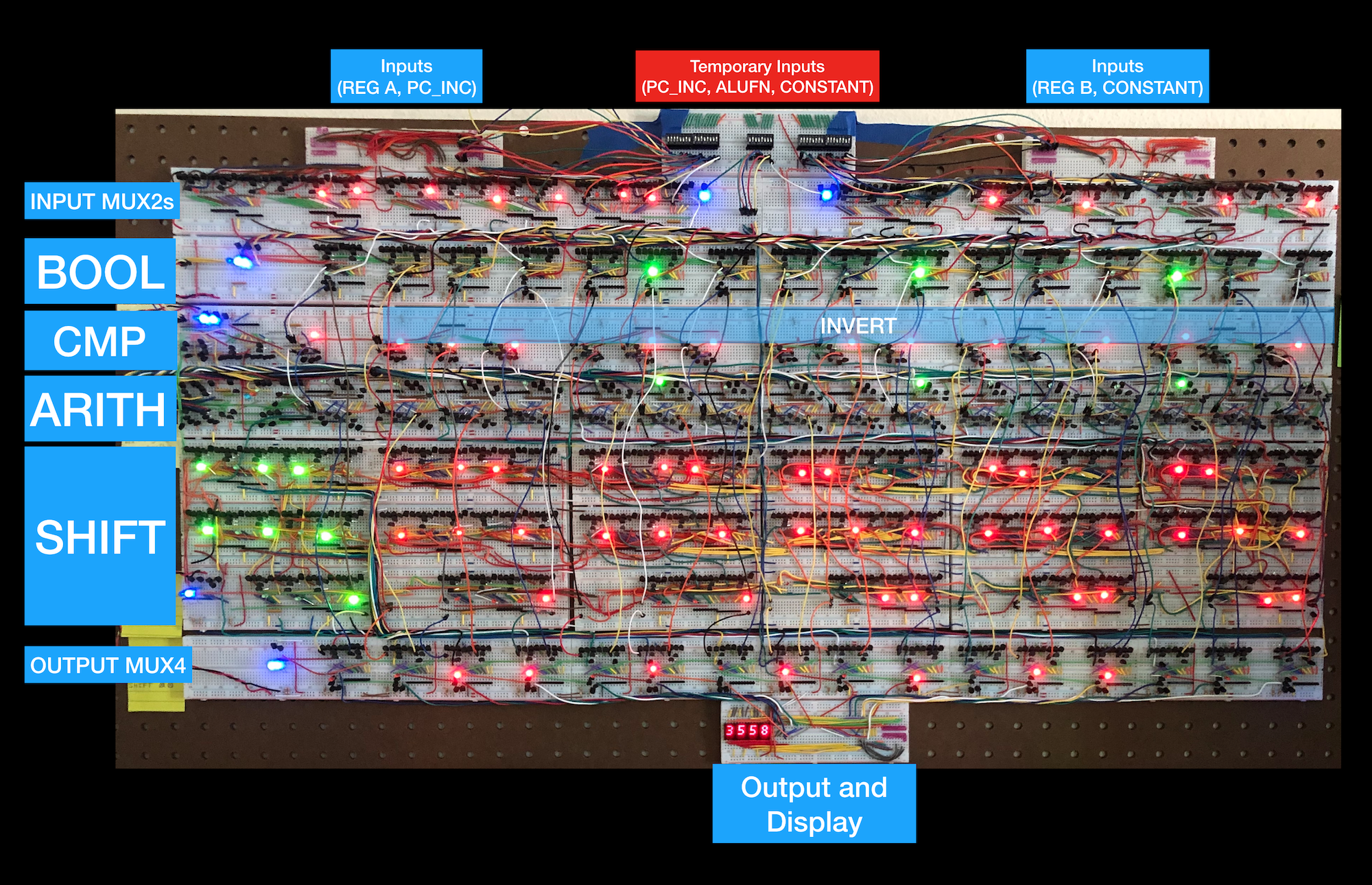
Putting everything together, here's the entire ALU pegboard, annotated:
![]()
The Spikeputor
I am building a computer featuring a 16-bit RISC CPU made of discrete transistors for learning, fun and art. It will be pretty large.