 Ted Yapo
I designed this circuit two months ago, but had no way to test it until recently. The goal was to create a 350 ps differential strobe pulse for driving a diode sampling gate (a 1 GHz bandwidth sampler). I populated the board late last night, and it only took an hour this morning to figure out one of the ICs was backwards :-)
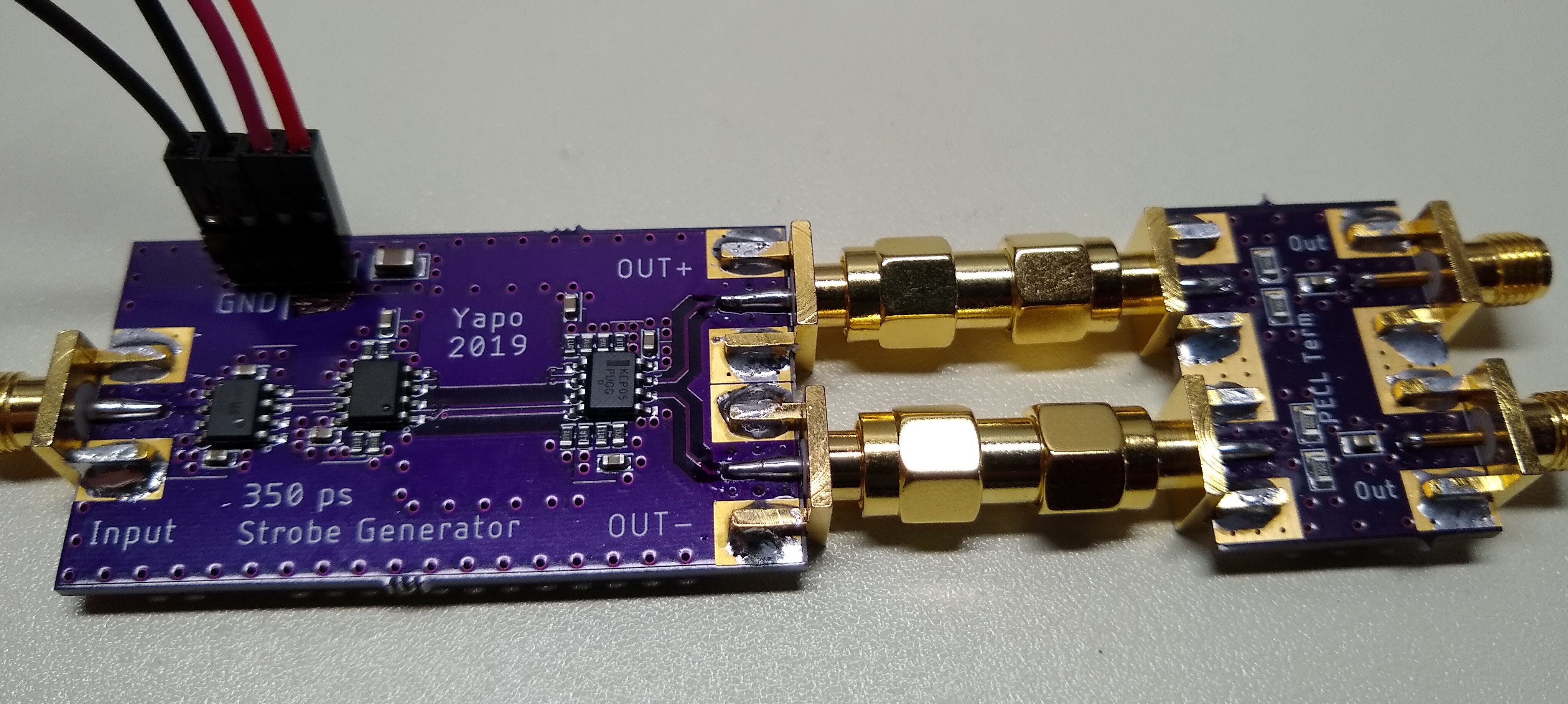
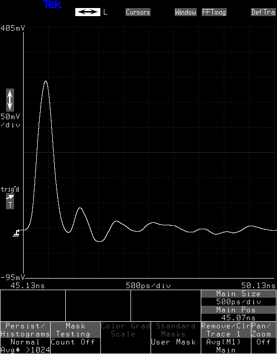
The board on the right is a termination so that I can look at the output with a 50-Ohm oscilloscope input. Shorting the PECL outputs directly into 50 Ohms tends to burn them out :-) Even with the seemingly short interconnects here, this still generates some reflections, which you can see in the second trace below. Those SMA adapters aren't short from the circuit's point of view.
The Pulse
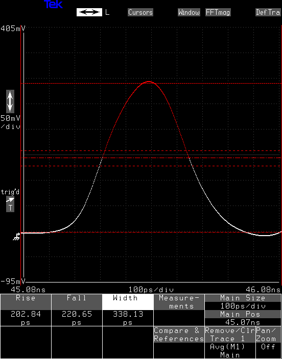
So, here's the output: a 338 ps pulse. The silkscreen on the PCB says 350, so I'm only off by 12 ps, or 3.5%. I'm pretty happy with the result. The amplitude isn't calibrated correctly here, since the output is attenuated by the terminator and the trigger pickoff delay line - did I do a log about that yet? Anyway, the outputs are differential, so there's also a negative-going pulse similar to this one.
On a larger timescale, you can see the reflections caused by the poor termination. In the actual system, these lines would be properly terminated at the receiver, probably eliminating these bumps. In any case, these aren't likely to be large enough to bias the sampling diodes into conduction, so they don't matter, anyway.
The Circuit
The uses the difference in length between two differential pairs to determine the output pulse width. An SY100EPT22 translator converts the LVCMOS input into 3.3V LVPECL outputs. This output is duplicated by an SY100EP1U 2:1 fan-out buffer. The 20 ps maximum output skew on this part could account for my 12 ps error. The two outputs then feed into an MC100EP05 AND/NAND gate, but one of them is delayed by going through longer traces on the PCB. On each incoming pulse edge, the output goes high briefly, until the delayed signal comes along to turn it back off again.
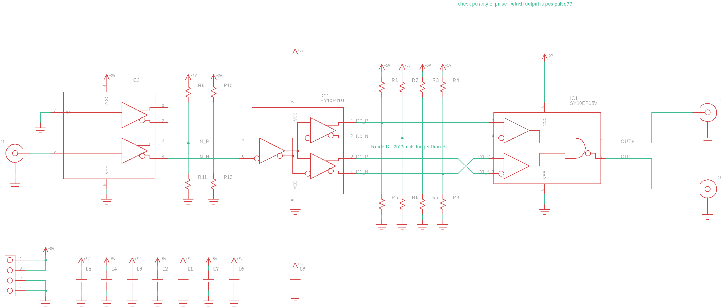
All of the pullups are 127 Ohms, and the pulldowns 82.5 Ohms, which is the Thevenin equivalent of terminating the lines in 50 Ohms to Vcc-2 V (for a 3.3V supply). The resistors dissipate more heat than you might expect - unless you've done the math, that is.
The output driver has a typical rise/fall time of 220 ps, which ultimately limits the minimum pulse width. You can try to make it shorter than this, but then the amplitude of the pulse starts to drop.
The Delay Lines
Here you can see the lines that determine the pulse width. The red traces are on the top of the 4-layer PCB, while the blue ones are on the bottom.
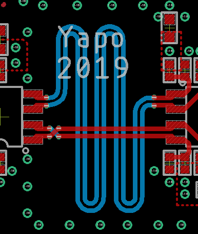
With a dielectric constant of 3.66, the OSH Park 4-layer process should have a velocity factor of 0.523, so signals should travel at 1.568e8 m/s. This is equivalent to a delay of 162 ps/inch. The shorter red pair is 492 mils long, while the longer blue one is 2643 mils long, for a difference of 2151 mils. This equals a delay of 348 ps, so hey, I'm only really 10 ps off!
So What?
The original plan was to use a pulse generator like this for a sampling head strobe. I'll probably still build one using this design, but have shifted my attention to pulse generators using inexpensive laser diode drivers instead. The PECL gates on this PCB are expensive, power hungry, and ultimately too slow for where I want to go. As a demonstration, it's not bad, and it's probably still worth developing into a full sampling head just for the experience, but there's no future in it.
On the other hand, this board validated a bunch of assumptions and techniques that I'll need later.
Discussions
Become a Hackaday.io Member
Create an account to leave a comment. Already have an account? Log In.
BTW looking at the routing, the red diff pair breakout could have been done from inside the chip and escape through the opening to avoid the via and cross over.
Also when you switch layers, you are supposed to place ground via nearby for any unbalanced current to return. There is a tiny bit of unbalance current as the pair of drivers aren't completely symmetrical.
There is also the fun part trying to balance the delays if your traces are on different dielectrics. e.g. FR4 (glass heavy) vs pre-preg (epoxy heavy). They both could be done on the red layer.
Are you sure? yes | no
Yeah, that's a good suggestion about avoiding the crossover on the red pair, although there are the terminations for the previous IC that kind of get in the way. I bet there's room.
I think the blue traces are the only really legit ones. PECL signals are referenced to Vcc, not GND, and the blue ones are the only ones run over a Vcc plane. With enough bypass caps spread around, it doesn't matter as much, but still.
Are you sure? yes | no
Last time we had to fix a vendor timing issue (pre-released part doesn't match datasheet), I cut microcoax cables to length as delay lines. I had made the suggestion of adding in a couple of resistors to swap the clock diff. pairs (inverse polarity = 180 degrees), but we needed finer adjustment than that.
Save a lot of time than to respin the board (only to find that vendor rev. their second batch of chips to finally match the timings.)
One of the old timers later on told me that's what Tektronix used on their scopes.
Are you sure? yes | no
The really old Tek scopes used lumped LC delay lines with center-tapped T-coils as the inductors - like hundreds of LC sections. There's a picture in Art of Electronics, 3rd ed. Later ones used special coax, also shown in the book. Here's the delay line out of a Tek 465 (100 MHz BW) that I just happen to have around for no particular reason ;-)
https://cdn.hackaday.io/files/1629986973706432/tek465-delay-line.jpg
I also have a couple of the Tek DL-11, which are 47 ns, 5 GHz BW (70 ps rise time) delay lines. They have a trigger pickoff before the delay so you can see the triggering event on the 11801 scopes, for instance. I haven't taken one apart yet, but that's next. Again, for no particular reason...
What kind of microcoax did you use? I bought some 1.3mm stuff at one point, and could not work with it at all.
Are you sure? yes | no
I used RG178B (1.85mm) microcoax. I had some 0.8mm samples from Samtec, but they are too lossy for what what I needed. I used the 0.8mm stuff for a 600+MHz protoboard.
http://suddendocs.samtec.com/notesandwhitepapers/tcf-3850-xx-xx_datasheet.pdf
Microcoax pig tails for WiFi are easy to get on aliexpress.
Are you sure? yes | no