 Ted Yapo
I just prototyped a stroboscopic A/D converter. It works, and it appears that you could make a similar one with available parts that would function as a 10 GHz sampling oscilloscope. This is where it gets interesting, people.
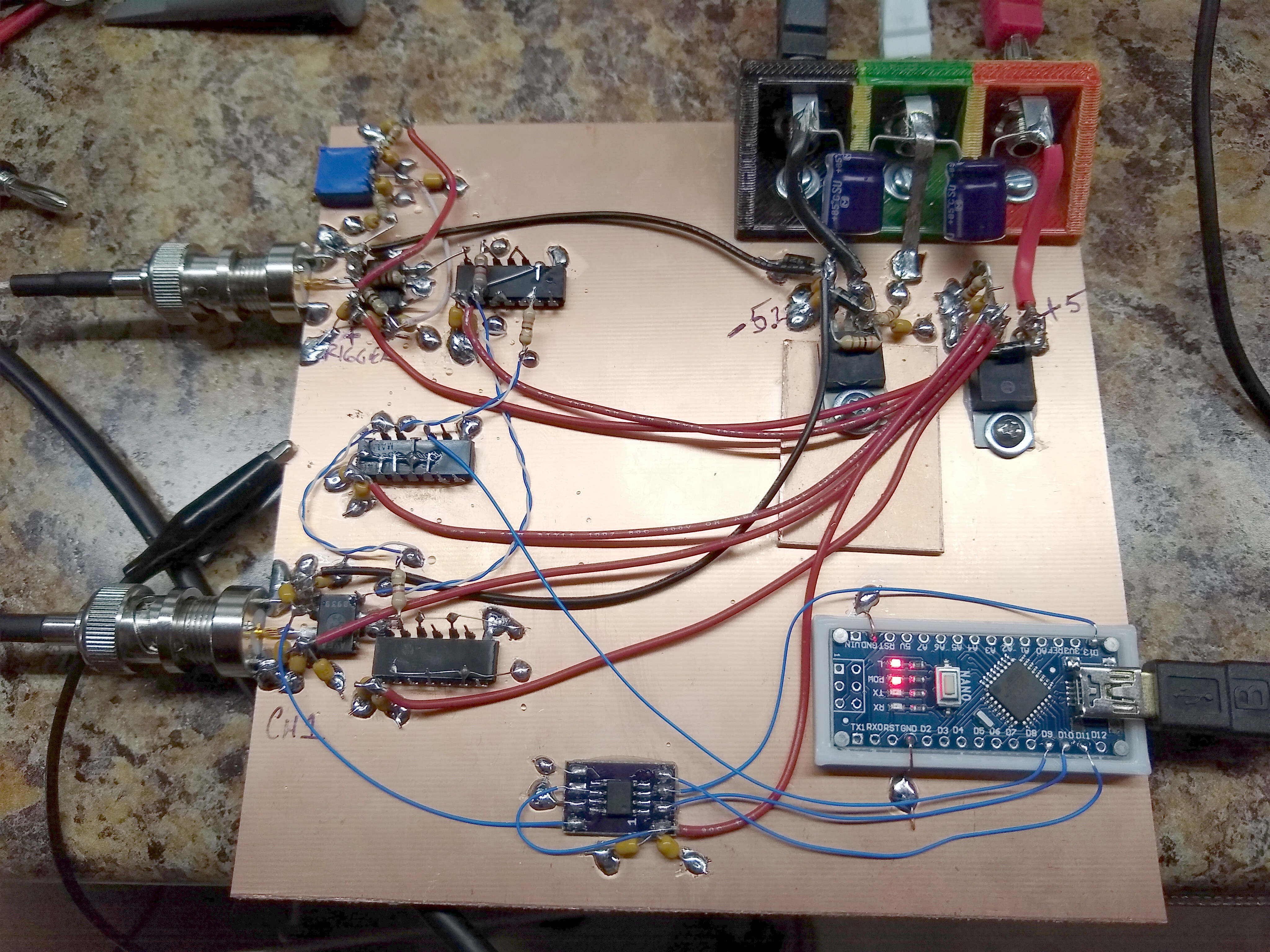
This version won't do anything near 10 GHz, but works as a proof-of-concept, and I was able to build it with parts I had on-hand. I love that kind of project.
Stroboscopic Converters 101
A stroboscopic converter looks a lot like a successive-approximation ADC (SAR ADC). If you consider just the DAC and lower comparator in the figure below, you can see the elements of a simple SAR ADC. Assume for the moment that we apply a DC voltage to the Ch1 input. We can read the value of that voltage by successively comparing it to different voltages output from the DAC. A naïve implementation would simply scan through all possible DAC output voltages, taking at most 2n tries for an n-bit DAC. You can do much better than this using a binary search over the DAC levels, of course, taking only n tries. SAR ADCs are cheap and accurate for low- to medium-speed ADCs, so are seen in many commercial offerings.
We've made a voltmeter. Now we need to turn it into an oscilloscope.
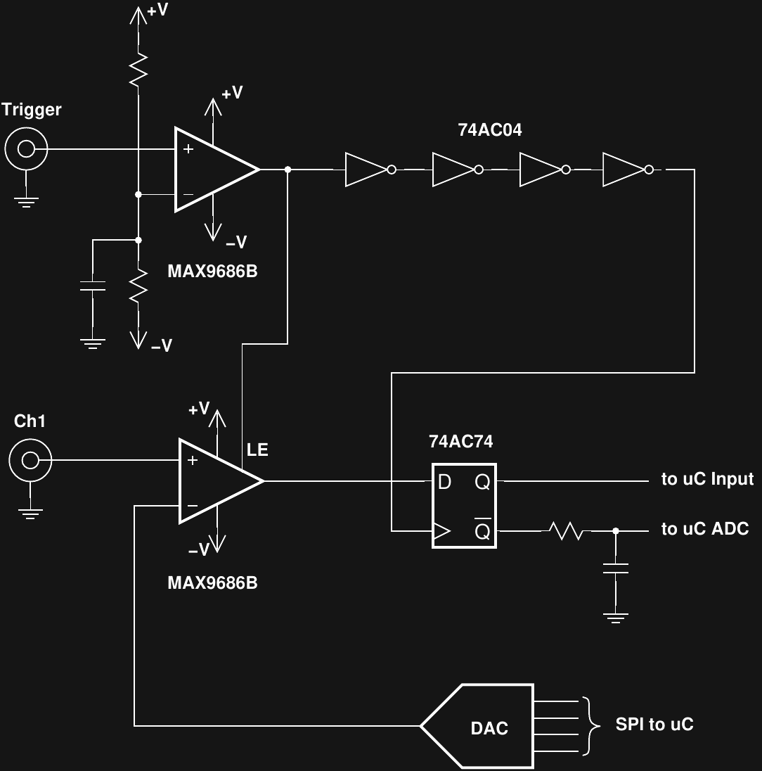
A closer look at the lower comparator reveals a latch-enable input (LE), allowing the voltage to be compared at a specific instant in time. To digitize an AC signal, a trigger pulse enables the lower comparator repeatedly at the same point in the waveform cycle. At this point, the motion of the input signal has been frozen, as if by a stroboscope, and the SAR conversion can proceed as normal. Once that particular data point has been digitized, the trigger point is moved slightly in time, and a new data point is captured. Doing this repeatedly results in a set of voltage measurements vs time, which is exactly what an oscilloscope does.
The schematic is a bit simplified and differs from what I actually built. For example, I needed 74ACT parts, since the comparator output is TTL level, which can't drive 5V CMOS inputs. All I had were 74ACT14's, so those went in for the 74AC04.
More importantly, a variable trigger delay is missing from the diagram. This part is critical to be able to reliably sample the input signal at specified points in time. In the prototype, the time scanning is faked by generating appropriate trigger points with arbitrary waveform generation software. For a real system, a variable delay line will need to be implemented. Luckily, such parts are made for very fine timing adjustments to critical clock and data lines. For around $10, you can obtain a digitally adjustable delay line with 10 ps steps (and an analog fine tuning input). The delays will need to be calibrated for use in a sampling scope, but that's an issue for another time. I'm working on a prototype adjustable delay board now.
First Tests
I haven't finished an adjustable delay line yet, so I used two outputs of an FL2k USB-VGA dongle with the osmo-fl2k software to generate both the sampling trigger pulses and a test sine-wave input. That's what the arbitrary waveform generator from the previous log was all about.
I managed to get a decent first result, sampling a sine input every 67 ns.
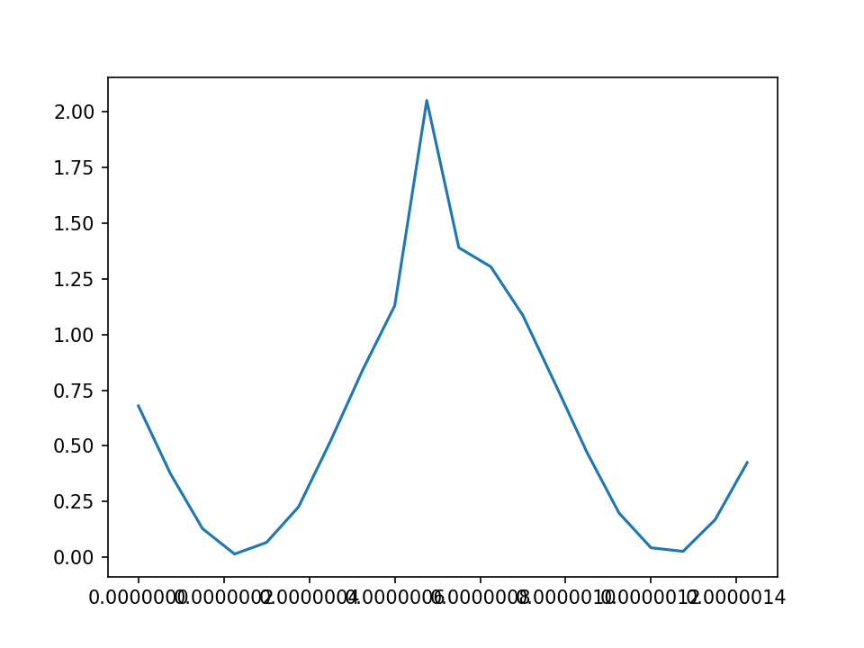
You can see where the successive approximation routine got stuck and produced a bogus conversion - clearly, there's a bug somewhere. It's not a bad first try, though. Now to go faster and faster and faster and...
References
This has been done before. A kickstarter from 2013 promised a 10 GHz sampling scope for $300, but didn't get funded. The clever folks over on eevblog eventually recognized this as a stroboscopic converter design, with an older version using ADCMP582 comparators (8 GHz input bandwidth). That design wasn't open-source, and appears to have been lost, so it makes sense to re-invent the (free) wheel in this case.
Next Steps
I'm still experimenting with a more traditional diode sampling gate. The difficulty is in generating the sampling current pulse needed to turn the gate on for a short sampling period. Modern parts can generate very sharp edges, but offer only small voltage swing, engineered to reduce EMI. This reduced swing has difficulty turning on the Schottky sampling diodes, though. Traditional diode sampling gates used step recovery diodes (diodes again!) to generate the pulses. Step recovery diodes are still available, but border on being unobtanium, so I'd like to avoid them if possible. More research is needed.
I'm going to pursue the stroboscopic converter angle in parallel with the diode sampling approach. There are a few faster comparators on the market which could get the bandwidth up to 10 GHz. Unfortunately, these are very expensive, so I will probably take an intermediate step, shooting for maybe 1 GHz bandwidth at first.
Discussions
Become a Hackaday.io Member
Create an account to leave a comment. Already have an account? Log In.