 Ted Yapo
One of the ways forward on this project is using diode sampling gates. Schottky diodes that can switch well into the tens of GHz are readily available, so it's just a matter of connecting them to the right stuff :-) I started out with a toy version - not that the 1N5711 diodes aren't capable, but the layout and pulse generator limit the circuit to lower frequencies.
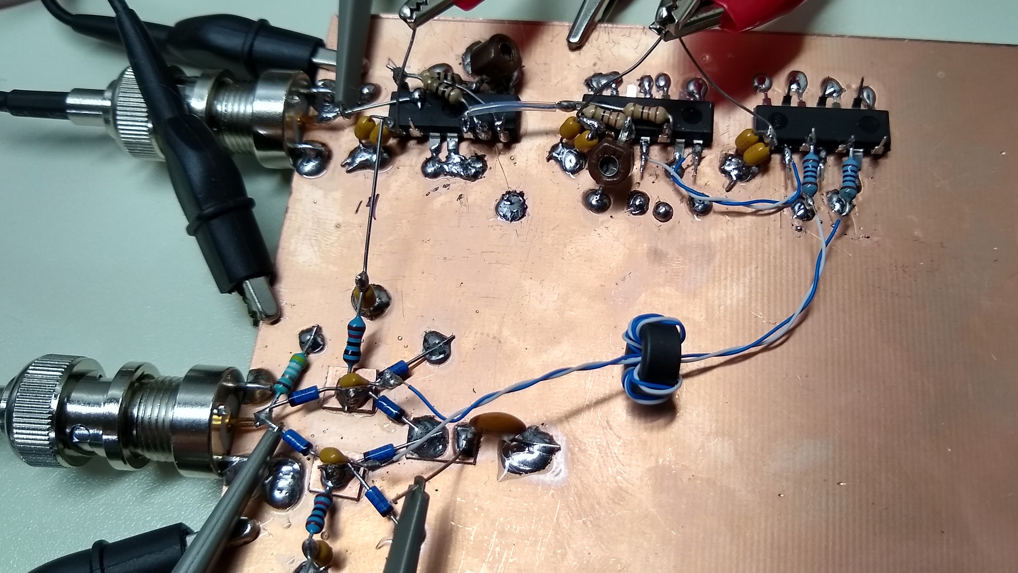
The business end of the sampler uses six 1N5711 diodes: four in a bridge, and two to clamp the reverse voltage.
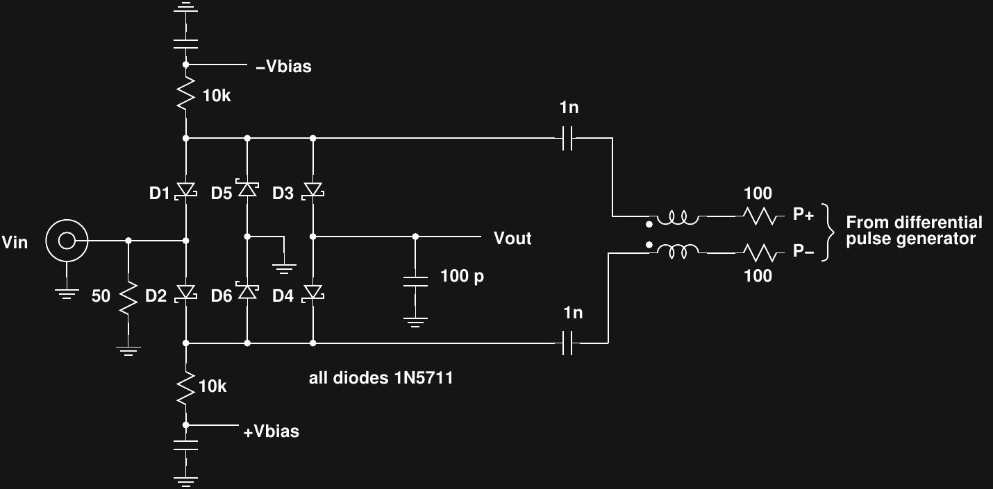
In the real thing, you'd use matched pairs (or quads) of diodes in SMT packages, but these work OK for breadboarding. I selected the six diodes from a lot of 50 by choosing ones that had about the same forward voltage. D1-D4 form a sampling bridge which is biased on during the brief sampling pulse. Between pulses, D5 and D6 clamp the voltage on the bridge to enhance isolation between the input and output. Ideally, these would be biased with split supplies, but for the initial tests, I left the bias supplies disconnected.
During the sample pulse, the 100 pF output capacitor sees the input voltage through the forward-biased diodes in the bridge and charges toward the voltage. The RC time constant of the circuit is based on the input impedance of 25 ohms (50 ohm source impedance in parallel with the termination) and maybe 10 ohms through the diodes. Combined with the 100 pF capacitor, this is around a 3.5 ns time constant. It doesn't matter that the capacitor doesn't charge fully during the strobe pulse, so this RC time constant doesn't set the front-end bandwidth. We can sample the waveform at the same point repeatedly until the capacitor settles to whatever resolution we need. This also does a lot of noise reduction by averaging.
I am also considering using a buffered version of the output voltage to boostrap the midpoint of D5/D6 instead of grounding it. You see this in some sample and hold architectures, but I'm not sure it's entirely needed yet.
The differential sampling pulse comes from a previous log, repeated here for convenience:
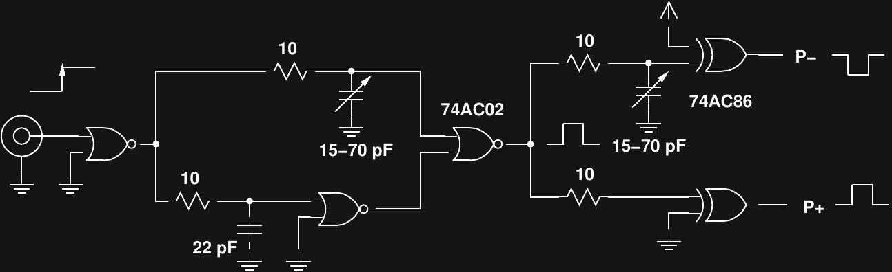
The rising edge of the input pulse creates a brief (approx. 2 ns) differential output pulse. A 2 ns sample pulse should create a sampler with around 200 MHz of bandwidth, although I haven't been able to test it that far yet.
Initial Tests
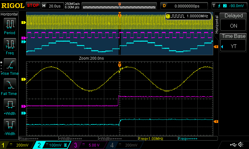
I was able to test the sampler using two outputs from a DDS signal generator: one output is the signal to sample, while the second output generates the sample clock. Here's an example of how it works:
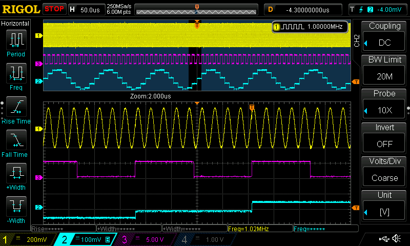
The yellow trace is the input waveform: a sine wave in this case. The magenta trace is the sample clock. At the rising edge of the sample clock, the input voltage is sampled and stored on the capacitor (cyan trace). You can see in the upper traces that the output is a "slowed-down" version of the input, since the sampling clock has been chosen to be slightly longer than 1/10 of the input period. In a real system, a trigger circuit and delay generator would create the sampling clock.
In the expanded traces (bottom), you can see how the output voltage changes in steps at each edge of the sample clock.
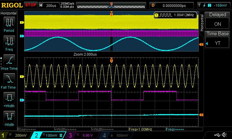
Sampler Kick Out
In this image, you can see the sampler "kick out," or perturbation of the input signal that happens during the sample pulse (lower yellow trace, directly under the trigger marker). This pulse feeds back into the measured system, which can be problematic. However, this kick-out can also be used to characterize the impulse response of the sampler. This may be useful later on.
More Resolution
From the above figures, it would be easy to mistake the sampling quantization with amplitude quantization and assume only coarse output steps can be created. This is not true; the examples above are simply to illustrate the behavior of the sampling gate. With a different sampling rate, a high-resolution version of the output emerges.
Output Offset
If you look carefully at the upper cyan traces in these images, you can see that two of them have a DC output offset. These were captured without the common-mode choke in the sample line. It turns out that the kludgy differential pulse generator doesn't create very symmetrical pulses, so there is a common-mode pulse along with the differential. This common-mode pulse gets rectified by the diodes to create a DC offset on the output. The solution is a transmission-line transformer made by wrapping the twisted pair line a half dozen times through a type 43 ferrite core. This common-mode choke allows the differential component of the pulse to pass, while blocking the common-mode pulse. The result is a zero-centered output.
This was a lucky guess on my part, but adding the transformer worked like a charm.
I probably should also add a manual offset adjustment. Every sampling gate circuit in old oscilloscope manuals seems to have one.
Next Steps
I have a PCB version of a similar circuit I actually build a few weeks ago, but never got working quite right. Now, having seen a diode sampler work, it's time to go back and debug that board.
It's also time to see if CML or PECL differential outputs have enough swing to turn on the diodes in this sampler.
Discussions
Become a Hackaday.io Member
Create an account to leave a comment. Already have an account? Log In.