 Ted Yapo
Of course, jitter will be around three orders of magnitude larger, but it remains to be seen what accuracy can be obtained by averaging many measurements. Wait, I'm getting ahead of myself. This PCB is a digitally-adjustable delay line built around an SY89296U programmable delay IC. This part, designed for adjusting clock edge timing, has a 1024-step digital delay control with 10 ps resolution, plus a 40 ps analog trim voltage input. I drive the trim voltage with a 12-bit DAC, allowing a theoretical delay step size of 20 fs. There will be non-linearities and jitter which limit the usable resolution to much greater step sizes.
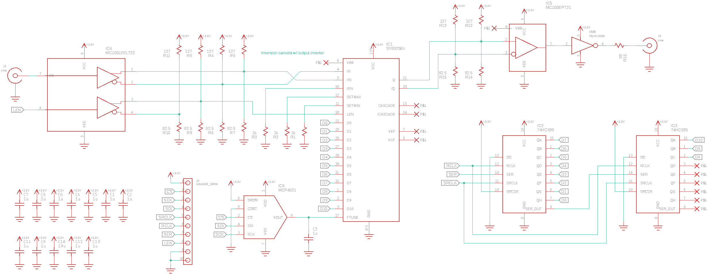
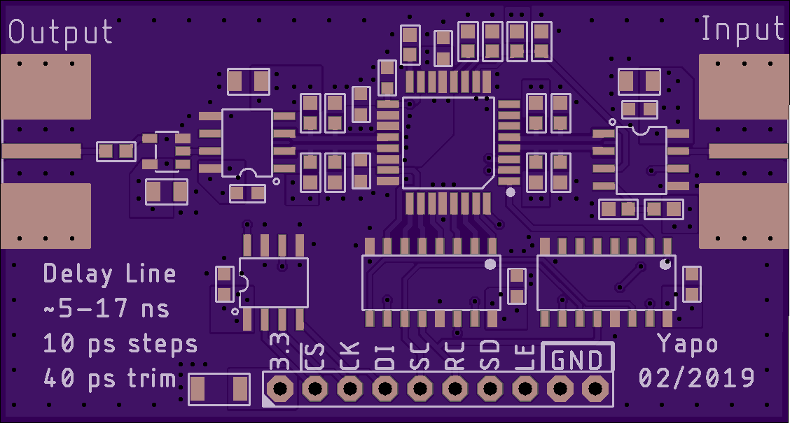
The board has two 74HC595 shift registers to hold the 10-bit delay control word, plus a MCP4821 12-bit DAC for generating the fine-tuning voltage. Since the delay IC uses LVPECL signalling, LVCMOS translators are used on the input and output. This is really nothing more than a breakout for the SY89296U.
Resolution
The SY89296U has 1024 nominal 10 ps digital delay steps, with less than 10 ps total jitter (2 ps cycle-to-cycle). It additionally has an analog fine-tuning voltage input with a resolution of 40 ps/V. I drive this input with a 12-bit converter with 0.5 mV step sizes, allowing for a minimum step size of 20 fs. This 20 fs number is somewhat meaningless, since it will be swamped by other issues.
Jitter
The SY89296U has a maximum 10 ps total jitter. One of the translators has 5 ps, the other has 2 ps. I don't know about the 74LVC04 inverter at the end; I suspect it has around the same. I might be looking at 15-20 ps total jitter through the whole chain. That's not too bad, and the results can be improved by averaging over many measurements.
Accuracy
The accuracy of the generated delays depends not only on the resolution and jitter, but the calibration of the SY89296U. The actual delays generated can vary by about 20%, according the the datasheet. So, I need a way to calibrate the delays. So far, the best answer I have is another PCB I just sent out which has dual TDC7200 time-to-digital converters. This should be able to measure delays with 55 ps resolution and 35 ps standard deviation; it's possible I can achieve better results by averaging over many samples, but I'm not sure how far I can push it.
I'm also wondering about other ways to calibrate the delays. Any suggestions?
I think I need to dive into the literature at this point.
The PCB
This was a new one for me. The LVPECL parts require special care and feeding, with their impedance-controlled and terminated differential traces and being referenced to Vcc instead of GND. I went with a 4-layer PCB, obviously. I don't mind paying extra for the 4-layer job at OSH park, I just wish there was a super-speedy option for this stackup.
Hey everyone, order more 4-layer PCBs, so they'll do one.
This PCB has been ordered as of 2019-02-09.
I don't think I've ever used the word femtosecond before. It's kinda fun.
Discussions
Become a Hackaday.io Member
Create an account to leave a comment. Already have an account? Log In.
Can you share the OSH park link? I would like to buy 3.
Are you sure? yes | no
I'm reluctant to share the design at this point since there is an error that requires cutting a trace - at least that's how I got it to work. The issue still isn't worked out completely in my head, because from the datasheet, it appears that it should work as designed. This was a quick breakout to get some experience with the part, and it was good enough not to spend any more time on :-)
If you need three of them, and are willing to deal with the minor re-work the PCB needs, I can send you the zipped gerber files to upload to OSH Park and order. If, on the other hand, you don't need three of them, I can send you one for free. I have two extras just sitting here - I got what I needed from the one I populated.
Are you sure? yes | no
Hi Ted - thanks for the reply. I acutally only need 1, but mentioned 3 due to OSH parks minimum. One for free would be great, but sending me the zipped gerber files is also fine - whatever is best for you.
Are you sure? yes | no
@Donnie Agema sent you a private message
Are you sure? yes | no
Hi Ted. I received the PCB you sent me today. Thanks again! Comparing the PCB with the schematic, it looks to me like the trace cut problem is due to the trace actually going to pin 6 of MC100EPT21 instead of pin 3. I will try to verify that when I receive the parts needed to assemple the board. I will let you know when done.
Are you sure? yes | no
@Donnie Agema You mean the MC100LVELT22? I think it does go to pin 3 as intended, but that part has the opposite orientation from the other SOIC8 on the PCB. See the layout here:
https://cdn.hackaday.io/files/1629986973706432/delay-pcb-layout.png
But, this exercise reminded me that when I assembled the PCB, I installed that part backwards at first! Nothing worked, of course. When I realized and installed it properly, pulses started coming through. Later, I realized I couldn't control the delay, and between debugging the software (which I still have to send you), and the rest of the PCB, I forgot I had originally screwed up the placement. It's entirely possible that I fried just one gate in the MC100LVELT22.
Next time I'm in the lab (looking like Weds at this point), I can check the PCB for evidence of this, and swap the part for a fresh one, and re-connect the trace. It's possible the board was OK as designed.
Are you sure? yes | no
Ah, yes. I did mean the MC100LVEL22. In any case, I see on the PCB that die voltage divide resistors to not populate go to the opposite side of the chip respective to the LEN trace (pins 3/6, whaterver way the chip is mouted). That does not agree with the schematic.
Are you sure? yes | no
There are really two LEN signals on the board for the two different logic families. The signal/trace named "LEN" is the external LVCMOS version of the PECL LEN input to the delay line. This LVCMOS version gets converted to LVPECL levels appropriate for the delay line by the translator IC. The LVCMOS version shouldn't be connected to the termination resistors, which are for the LVPECL signals. The LVPECL version of the signal is named "N$18" -- not a great choice, perhaps, but distinct from the other one.
I am not sure why they opted to use LVPECL levels for the LEN input in the first place. It would make a lot more sense if LEN accepted the same LVPECL/TTL/LVCMOS levels as the D inputs. After all, the same logic that sets the data pins will know when it's OK to latch them. Maybe it actually uses these levels, and the datasheet is incorrect.
Are you sure? yes | no
My suggestion for calibration of delays would be to make a setup which will map delays to frequencies (e.g. incorporate delay in a ring oscillator), as measuring frequency can be quite accurate.
Or, measure phase difference between a stable clock and its copy delayed through the delay circuit.
In both cases the many measurements principles is immanent - it is a continuous repetition of delay measurements with averaging.
Are you sure? yes | no
Yeah, that's a great idea! I could use an external inverter to close the loop, and measure frequency vs nominal delay setting. The base delay might be around 5 ns. If I got an oscillator running at 100 MHz with this, a 10 ps step would change the frequency by 20 kHz, easily measured. Even a 20 fs step (hopelessly in the noise) would move the frequency by 400 Hz (4 ppm). I think.
Are you sure? yes | no