 Ted Yapo
I had some 2-layer boards made to test assumptions about coplanar-waveguide (CPWG) over ground plane traces. I also used this test to explore issues with SMA-connector footprints.

I understand that this is just normal "random" FR-4 substrate, whose properties can vary widely, but the CPWG structure doesn't seem extremely sensitive to dielectric constant changes in the substrate. It does appear to be sensitive to the soldermask, though, for reasons I'll get into below.
32/6 CPWG
I tested two CPWG geometries, both of which calculate out to 50-Ohms on (most) trace impedance calculators. The first, which seems relatively popular, has a 32-mil trace with 6-mil gaps to the top ground plane on either side; there's a solid ground plane on the bottom of the board. I also tested two different SMA footprints on these traces. One uses the same old footprint I had been using, which has a capacitive impedance bump due to the thick center pin of the SMA connector, while the other has some of the top ground plane cut away -- with a knife -- to compensate.
You can see a whole bunch of stuff in the annotated TDR trace below. Starting from the left, we first see the RG-316 cable, which measures out as 48.42 ohms (it's spec'd 50 +/- 2). Next, there's an inductive (positive) bump due to the mated SMA connectors. After that, there's the PCB footprint for the connector. In my old footprint, you can see a large capacitive (negative-going) bump, while in the cut-away version, you can see I removed too much copper. Back to work on that one.
The central flat portions are the traces themselves. Without soldermask, the trace measures 52.0 Ohms, while adding the mask brings it down to 48.4 Ohms. Both traces would have more than 34 dB return loss, and are actually within the tolerance for common "50-Ohm" cables, so they're probably equally fine for all but the most critical uses.
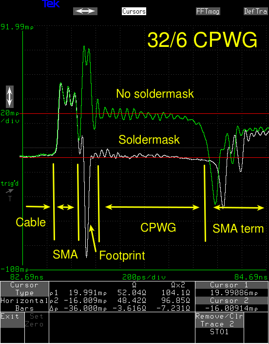
It's very interesting that the soldermask makes a difference of 3.6 Ohms in this case, though. I think what's happening is that because the ground plane is so far away in the 2-layer board compared to the side gaps (60 mils vs 6 mils), a lot of the energy is carried in the gaps rather than the substrate. So, adding soldermask with a dielectric constant of around 3 into the gap makes a big difference. I would expect the effect to be smaller where the gap-to-thickness ratio was smaller, like in 4-layer boards, or traces with wider gaps.
41/8 CPWG
Here's another CPWG structure that calculators put at 50 Ohms, this one with wider gaps.
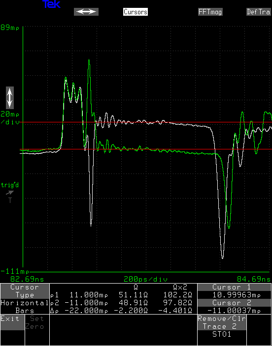
Again, the bottom trace is without soldermask and the top trace has it applied - ignore the trace colors, they are opposite from the plot above. As expected, the wider gap means that the soldermask has less influence on the characteristic impedance, in this case 2.2 Ohms vs the 3.6 Ohms for the 32/6 structure. Again, both these traces are perfectly good "50 Ohm" equivalents, so it really shouldn't make much difference. Unless your design rules don't support 6-mil gaps, there's probably no reason to use a 41/8 trace, unless you need a 41-mil wide solder pad for some component.
SMA Footprints
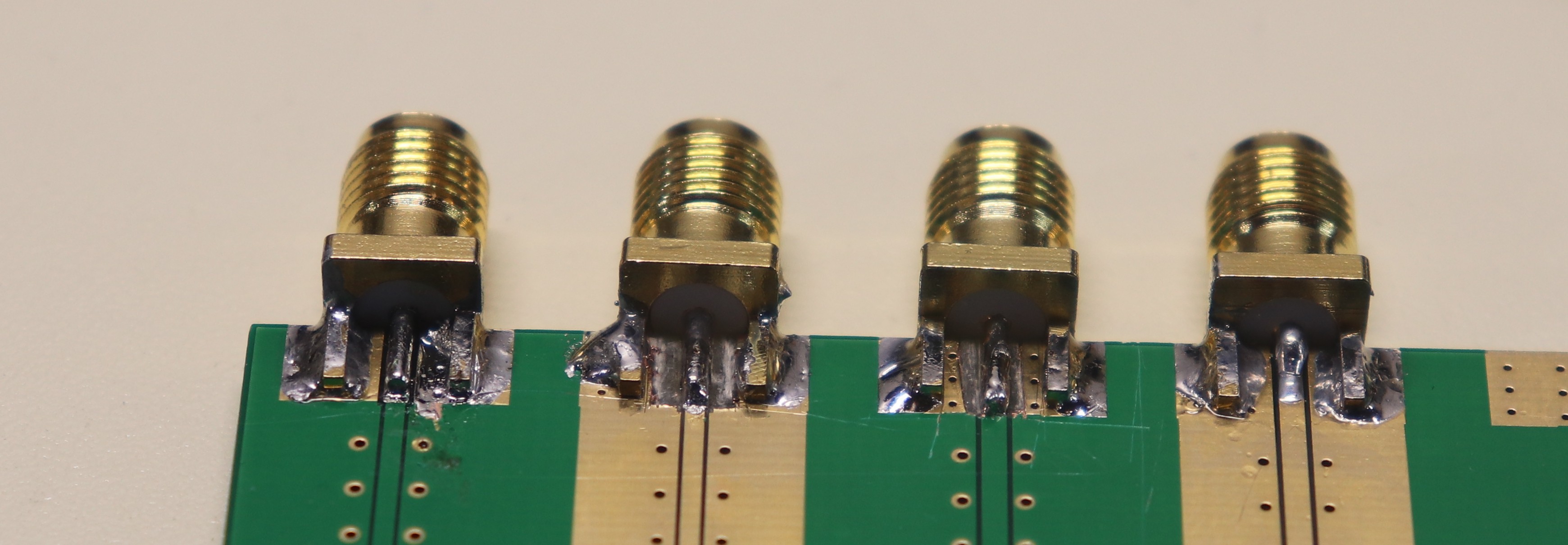
One of the places you might need a 41-mil solder pad is on edge-launch connectors. Some of them have wide pins that need a pad wider than 32 mils. The problem, though, is that the round pin itself introduces some capacitance. This can be seen as a dip in the TDR trace. For two of these tests (the outer SMA jacks on the left and right sides in the image below), I used my "standard" SMA footprint, which has a 41-mil wide trace for soldering the pin, and 8-mil wide gaps. Without the pin there, this is just the 41/8 CPWG tested above - you can see this on the rightmost jack, where the trace seems to got right to the board edge.
For the center two, I tried cutting away some of the ground plane on either side to widen the gaps. You can see in the traces that this has the intended effect - the capacitive bump was removed, and was replaced with a slight inductive bump. On the second try, I removed less copper, but it was still a little too much. In any case, this shows the way forward - I need to re-design the footprint with wider gaps at the sides. I don't know exactly how much, but I can guess and try again.
Or maybe get an openEMS simulation going.
Why not just make it perfect?
With the variability of FR-4 on 2-layer non-impedance-controlled boards, it would seem that chasing a better impedance match would be a waste of time, but at the moment I have nothing better to do, so I'll give it a shot. I'd like to get a good footprint designed, and a "standard" CPWG geometry, and then just be able to use them going forward.
Don't Do This
You might notice that I removed the soldermask from the SMA connector footprint. Never do this - it it incredibly easy to bridge the gap with solder, then you have to spend a long time cleaning it up. For this side of the PCB, I got smart and used some kapton tape to mask the traces, but the other side of the PCB is a disaster. You can see it in the header image at the top of this log.
Discussions
Become a Hackaday.io Member
Create an account to leave a comment. Already have an account? Log In.