 Ted Yapo
So, after evaluating all the parts I could find with fast edges, I've come to the conclusion that none of them are suitable for generating the strobe pulse required for a high-speed diode sampling head. The available parts - logic, comparators, and laser diode drivers - all have output swings which are too small. Time to use discrete transistors. At GHz speeds. Ugh.
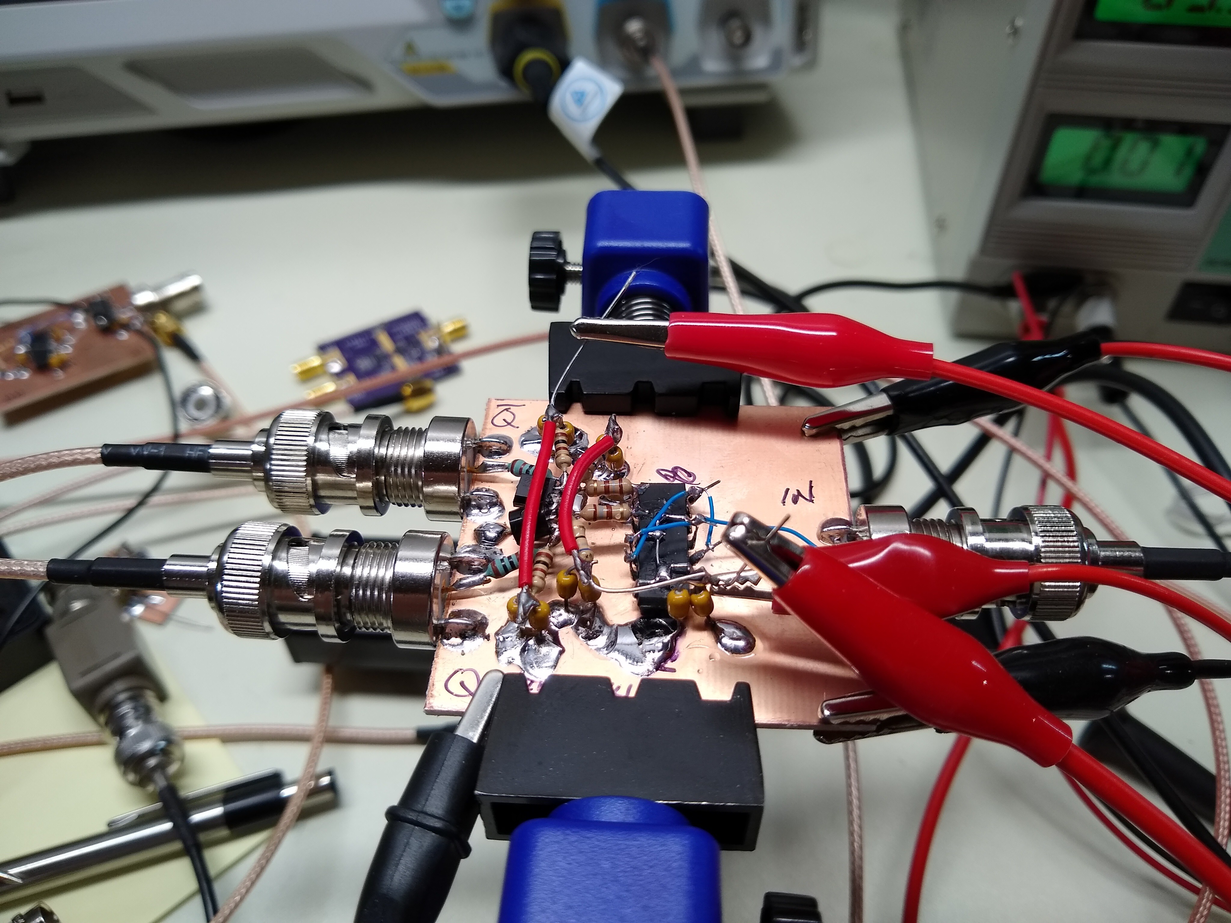
I started with what I had on-hand: a pair of KSP5179 transistors. They're rated at a minimum transition frequency of 900 MHz, which is around three times as fast as your ordinary 2N3904. Still, they won't do for the real sampling head. I'm looking at some 12 GHz ones at the moment, with 45 GHz SiGe units as a backup in case 12 doesn't cut it. For now, though, these T0-92 dinosaurs will serve as a proof-of-concept.
In the current plan, a discrete-transistor differential output stage will be driven by the output of a CML comparator.
Faking CML
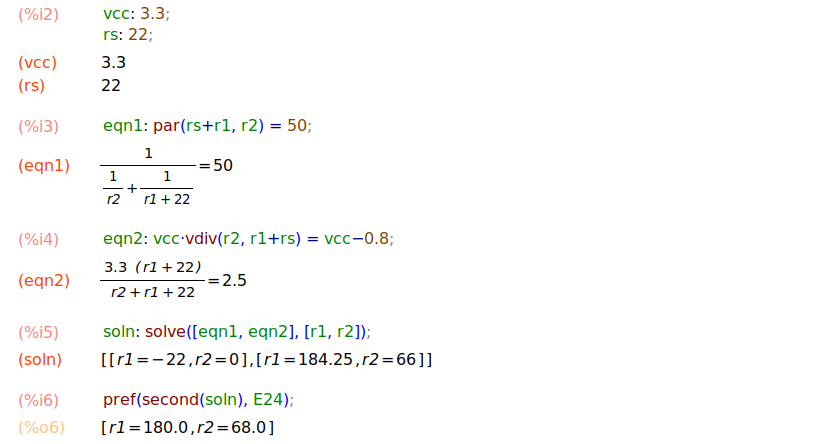
The first thing to do is to simulate a CML output swing without having to use a real CML part for testing. They're all blazingly fast, which would be wasted on these modest output transistors, and they only come in SMT packages. Instead, I added some resistors to transform the 0/3.3V CMOS outputs of a 74AC74 flip-flop into the 2.5/3.3V outputs (800 mV swing) of an unloaded CML output. The correct choice of resistor also provides a 50-Ohm output impedance like real CML. Those 180-Ohm and 68-Ohm resistors do the trick.
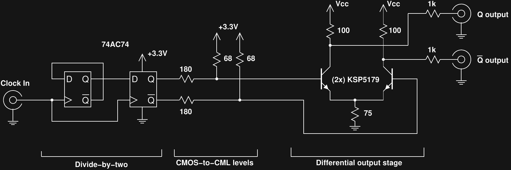
I calculated the resistor values based on an assumed 22-Ohm output impedance for the 74AC74. It's really lower than this, but close enough. Maxima made short work of the required algebra. This kind of thing used to mean a half-hour diversion, including re-doing the manual calculations to catch mistakes.
Differential Output Pair
The output circuit is very simple. The two transistors are arranged as a differential pair. The bases are driven by the CML levels. The 75-Ohm and 100-Ohm resistors set the output stage current and voltage swing. This is a textbook diff-pair and it just works. Parasitics are probably bad on this layout, but there's not too much that can be done with these big through-hole parts. The pair is powered by a higher voltage than the CML stage, so it can have a larger voltage swing. That's the key thing that couldn't be done even with open-collector laser diode drivers; there are always protection diodes in the way.
Measurements
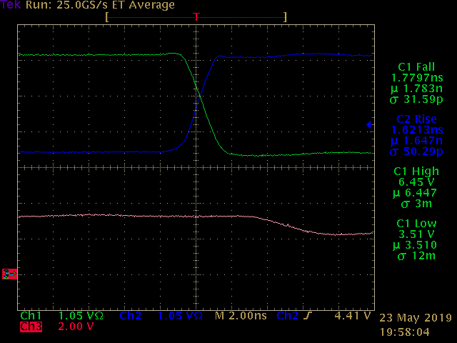
Here's what the output looks like. The top two traces are the outputs from the collectors of the transistors in green and blue. The bottom trace (pink) is one of the CML outputs - it's probed with a normal 10x probe with a long ground lead, so it shows some waviness. The rise and fall times of the outputs are around 1.7 ns. A rough back of the envelope calculation says that 12 GHz transistors might bring this into the 130 ps range, assuming everything else coöperates.
This test used a 7-volt supply at Vcc, and produces a single-ended swing of around 2.9 V (5.8 V differential). I figure I need around a 6 V differential swing to drive a diode sampling bridge, so this is very close. A little tweaking of the output stage resistors would do it.
The output, like the input, rides on a high DC bias voltage. That's OK -- it will be AC-coupled to the diode bridge. It's also important to note that the transistors must be kept out of saturation, in other words, the base voltage must be less than the collector voltage. On the screen, the red trace must be below the other two. You can see that the output supply voltage could be reduced a bit here.
The outputs have built-in 1k resistors to make 21x Z0- probes when combined with 50-Ohm scope inputs. Luckily, the scope allows you to enter any number for the probe multiplier that you like. Note the 1.05 V/division scaling :-)
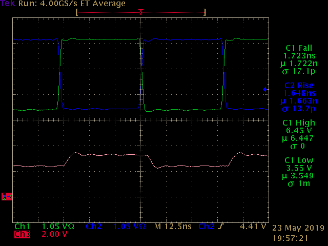
Zooming in, we can get a better look at the transitions. They're actually better than I would have expected - nice linear ramps.
Simulation
The KSP5179 datasheet has a SPICE model, so I simulated the circuit before building it.

The simulation output is a little different from what's observed on the real circuit.
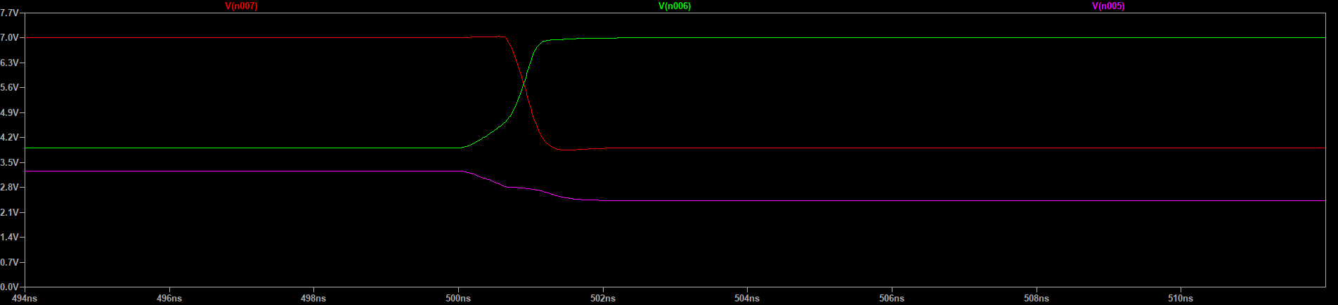
The falling outputs look qualitatively the similar, but the rising edge on the simulation hangs a little bit. If I weren't looking at the input voltage clearly lower at that point, I'd say this is a symptom of transistor saturation. I may play with the simulation a little more to see if I can determine what might be causing this - and why I don't see it in real life. Debugging the simulation seems strange, but it's worth figuring out what the difference is.
The predicted output swing is 3.1 V, while the actual circuit showed 2.9 V. Close enough.
Of course, there's a ton of parasitics from the layout not accounted for in the model. So, I'm not terribly worried that the simulation predicts transition times of around 400 ps instead of the observed 1700 ps. I am a bit interested, though. I'll be a little more concerned if things don't improve with some SMD transistors in a tight PCB layout, which is the next step.
Discussions
Become a Hackaday.io Member
Create an account to leave a comment. Already have an account? Log In.