 Ted Yapo
Someone asked me about making a short pulse generator -- a few ns width -- with CMOS levels. I had done some fooling around with this before, so I took the opportunity to play around a bit. Here's what I came up with:
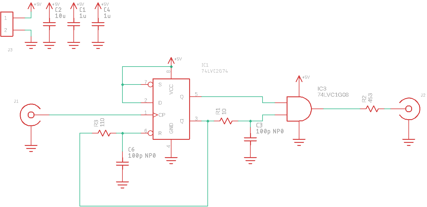
the idea is to use a 74LVC2G74 to trigger on an incoming rising edge. This sets the d-flop, since the D line is pulled high. An RC delay composed of R3/C6 delays the now low Q_bar output as it feeds back into the Reset_bar input of the flop. This will reset the flop after approximately 12 ns. Meanwhile, a second RC delay, R1/C3, delays the low-going edge of Q_bar into the AND gate. For the brief period that the AND gate inputs are both high, the output of the AND is high, generating the output pulse. The pulse width is a function of R1, C3, and the input and output characteristics of the gates involved, so some tweaking is in order to get the exact pulse width you desire. It's also important to choose NP0 capacitors so that the delays will be stable with temperature.
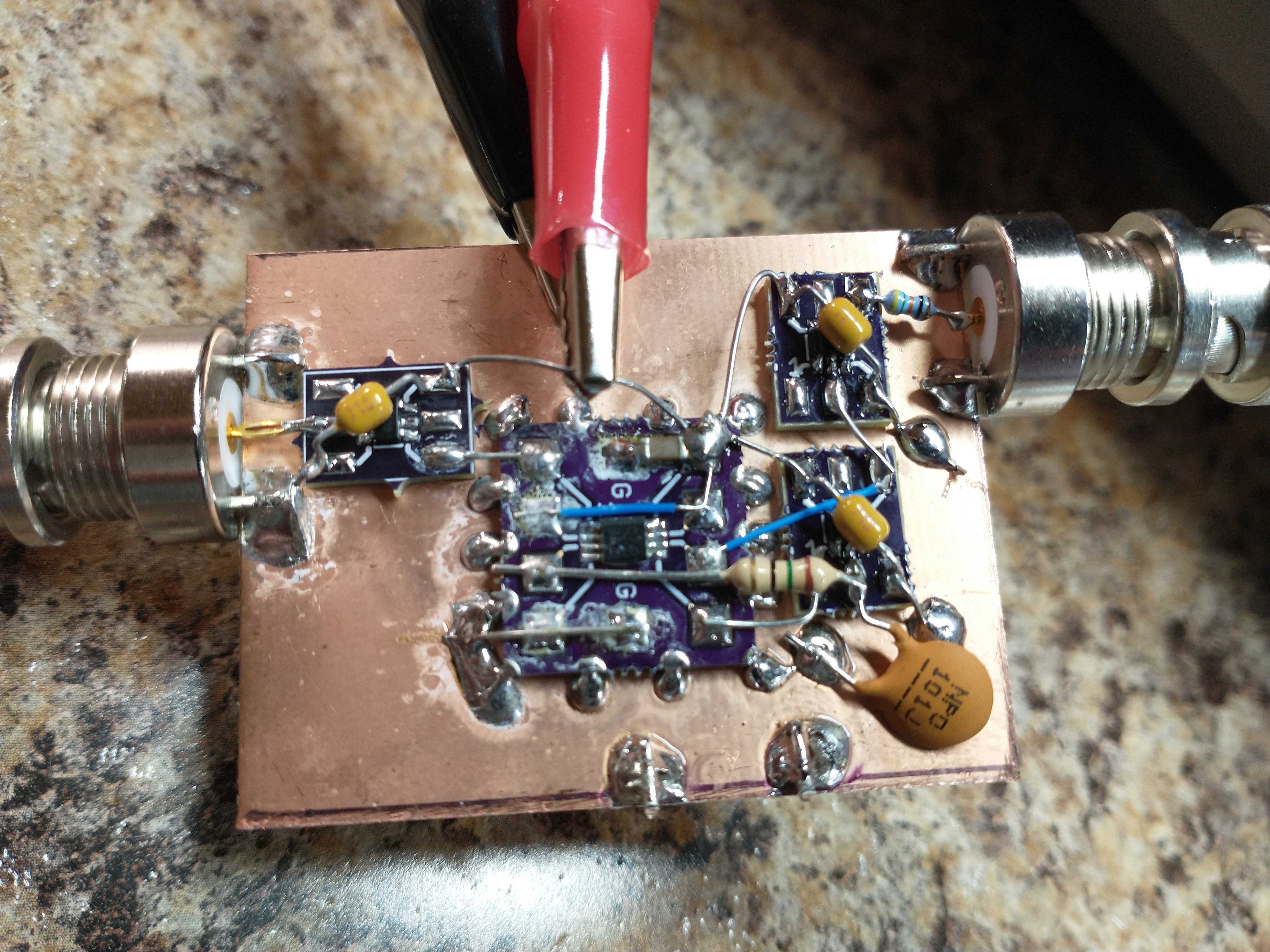
Here's an image of the prototype. I used a 74LVC1G00 NAND followed by a 74LVC1G04 inverter since I didn't have a 74LVC1G08 handy.
and here's the output (bottom, red trace), input (top, blue trace), and flip-flop Q output (middle, yellow trace)
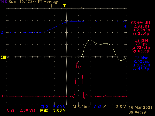
The input pulse is from my siglent arbitrary waveform generator, and has slow 9 ns edges. The output pulse is 2.992 ns +/ 52.4 ps long -- the goal was 3 ns -- and it has a rise time less than 650 ps. Remember, this was with a 74LVC1G04 output, so with the 74LVC1G08, the rise times may be a little different, but it will be well under 1 ns.
Note that the 453-ohm output resistor forms a 10x resistive probe when connected to a 50-ohm oscilloscope input.
UPDATE
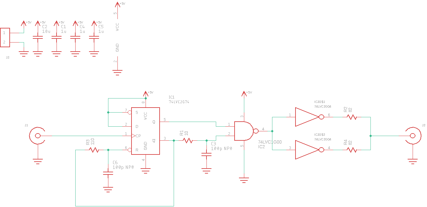
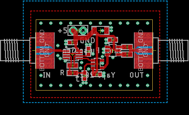
I designed a PCB to see what effect a proper layout has on the pulse shape. I also used a 74LVC1G00 followed by a pair of inverters from a 74LVC2G04 so that it can drive 50-ohm loads directly; a single 74LVC gate doesn't source/sink enough current.
and here's the layout:
in about a week, I'll be able to test it and see how it works.
UPDATE 20210323
The PCBs arrived today, but I had a difficult time with them. Once all the parts were soldered on, the board drew a lot of current, making me suspect a short. Some probing with a DMM showed one diode drop across Vdd/Vss, a sure sign of a backwards-connected IC. Sure enough, my footprint for the 74LVC1G00 was wrong, swapping Vdd and Vss. Oddly enough, I made this footprint a couple years ago for a project that never got off the ground, and it sat lurking in my library the whole time. Anyway, I reworked the PCB and got on with testing.
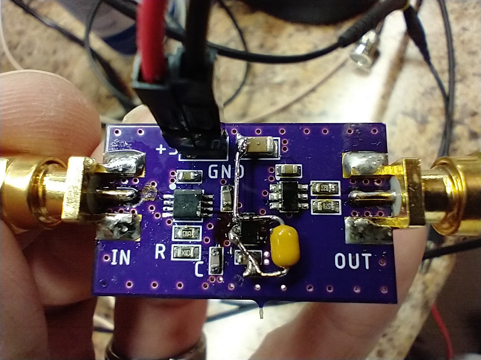
How does it work? About the same as the prototype.
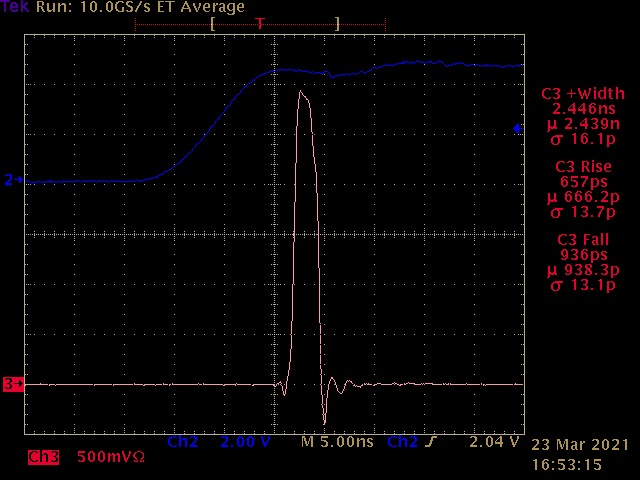
The input edge from a Siglent DDS is shown in the top trace, and the output pulse is at the bottom. The pulse width, as measured by the scope, is 2.4 ns, a little shorter than the prototype. There's less ringing at the top of the pulse, and it's also a bit shorter than the original. You could increase the 10-ohm resistor to stretch it a bit.
The repetition rate is limited by the reset pulse fed back to the flip-flop. Testing revealed that it can be driven at 59 MHz without issue:
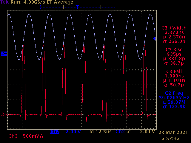
but at 60 MHz, every other edge gets dropped.
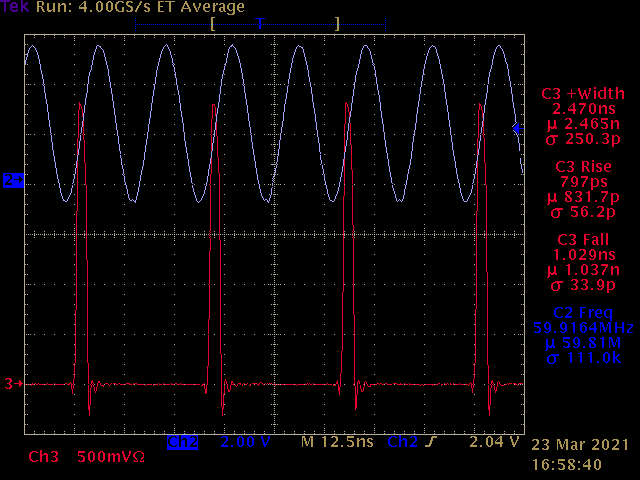
Note that the amplitude is also higher at lower repetition rates. Could it be that current draw of the output drivers is causing the voltage to droop? The output drivers are pushing 5V into a 100-ohm load -- a 50-ohm series termination plus the 50-ohm term inside the scope -- so, that's 50 mA. The 74LVC1G04's on the output can do 32 mA each, so that's OK, but maybe getting the power to them is the issue.
Also note that I'm driving the thing with a sine wave input here. My DDS only goes to 25 MHz for square waves.
Is the PCB version better? The overshoot on the falling edge is only around 500 mV instead of 1 V, so that's better. Plus, the paralleled output drivers can handle 50-ohm loads.
Discussions
Become a Hackaday.io Member
Create an account to leave a comment. Already have an account? Log In.