Ted Yapo
-
Coiled Delay Line
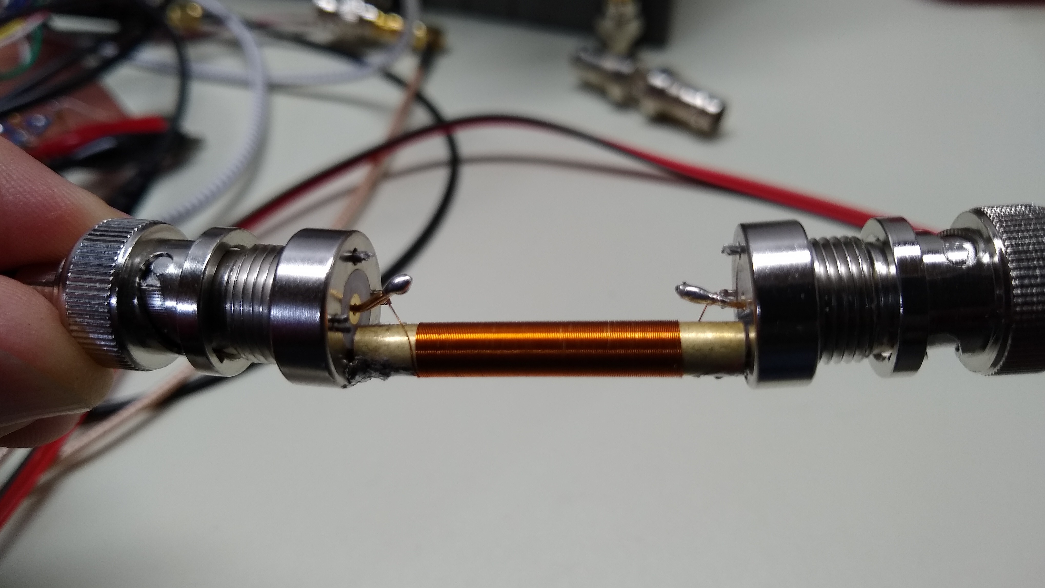
03/31/2019 at 03:57 • 3 commentsI was reading about coax delay lines today and was reminded about this kind of compact coiled delay line. It's essentially a coiled transmission line created by winding fine wire around a conductive tube. So, I made one - completely randomly - from stuff I had around just to see what it would do.
![]()
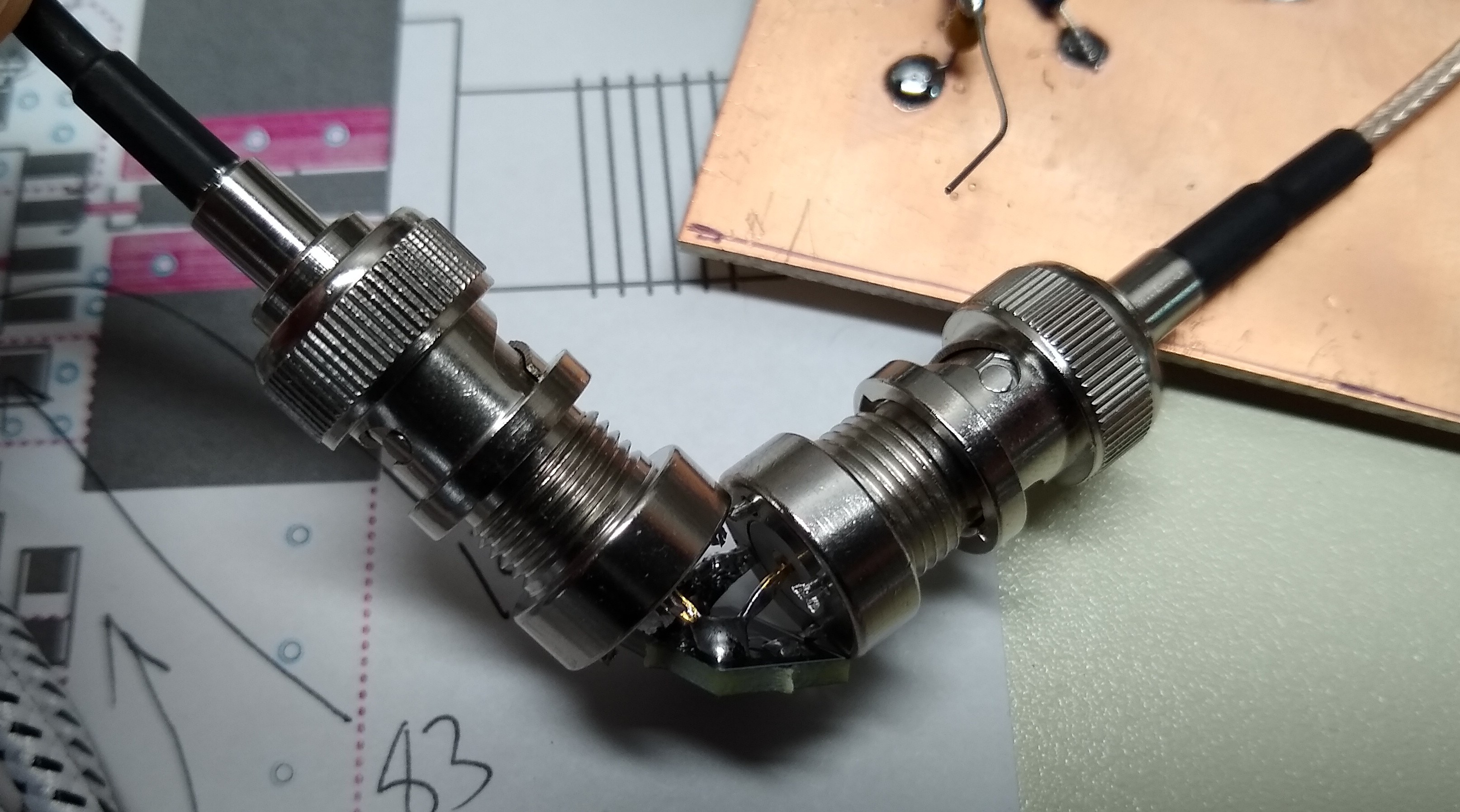
To make the assembly, I soldered a length of 4.8 mm diameter brass tubing between the ground lugs of two BNC jacks, then wound a length of #36 wire on the tubing. I don't know the exact length of wire or number of turns, but the coil itself is 24 mm long. Some calculations show that this should be approximately 2.93 m of wire.
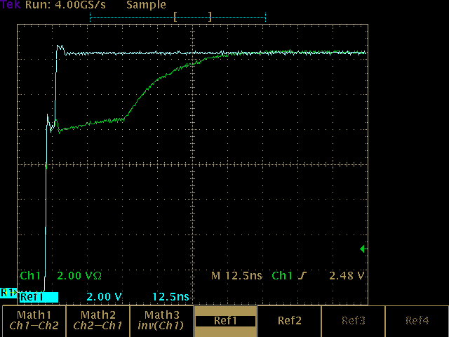
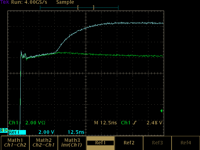
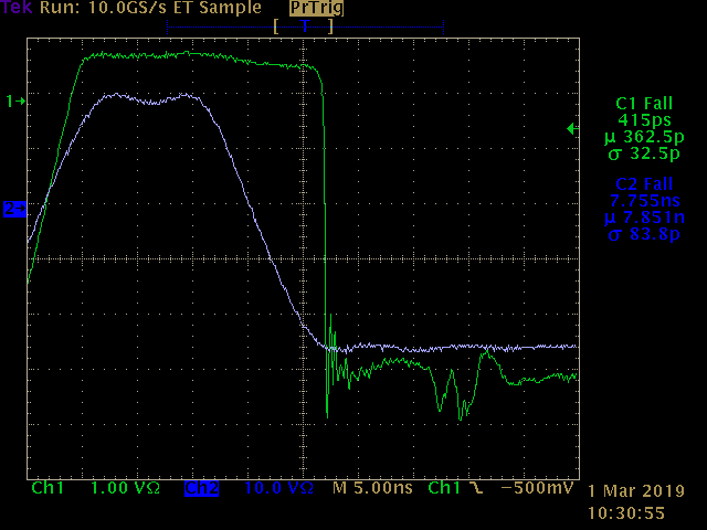
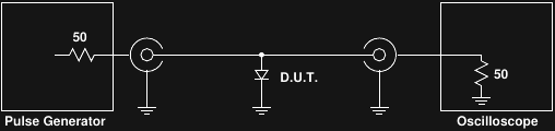
The first test of the delay line was to hook it up to an oscilloscope to measure the delay and bandwidth. The delay line feeds channel 2, while a reference pulse, identical to that going into the delay line, is shown on channel 1.
![]()
The delay on both the rising and felling edges is very close to 20 ns. This corresponds to a speed of 1.465 x 10^8 m/s, or 0.488 c in the wire. In the coiled structure, this is equal to 1.2 x 10^6 m/s or 0.004 c. That's pretty slow!
This delay is equivalent to 4.03 m of typical coax with a velocity factor of 0.66.
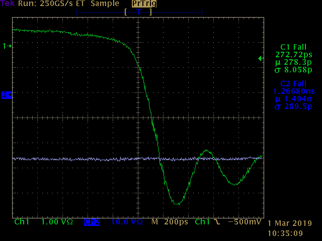
The bandwidth of the delay line can be estimated from the rise time of the pulses. Corrected for the rise time of the input pulse (9.25 ns), the output pulse has a rise time of 29.3 ns. This is equivalent to a 3 dB bandwidth of 11.9 MHz. Wow, that's not very good.
I'm guessing that the bandwidth is degraded by capacitance between adjacent turns in the coil. Maybe it could be increased by adding a little space between them.
When I get a chance, I'm going to measure the characteristic impedance of the line. Not quite sure the best way to do that yet. TDR or VNA?
TDR Tests
I fired up the #Tiny TDR this morning to test the characteristic impedance of the line. Here is a shot of the step from a 33 cm length of cable into the delay line. The Cyan trace (top) is the reference trace with just the cable connected to the TDR, and the green trace (bottom) is with the delay line connected. There is very little, if any, step at the boundary, indicating that the delay line has a characteristic impedance close to 50 Ohms.
![]()
Here it is on a longer time-scale where you can see the end of the delay line. From a TDR perspective, the end looks like it's terminated with a capacitor, although this also mirrors the rise-time measurements taken with the scope. There's some deep connection here that's evading me at the moment. Again, the cyan reference trace is the output cable alone; the green is with the delay line attached. At this scale, you can see some slope to the trace before the end of the delay line.
![]()
Finally, here it is without a 50-ohm terminator at the end of the delay line (cyan), and terminated (green). Again, it looks like little reflection from the terminator. You can still see some small rise and fall of the terminated trace, though. Maybe the impedance is a little higher than 50 ohms?
![]()
-
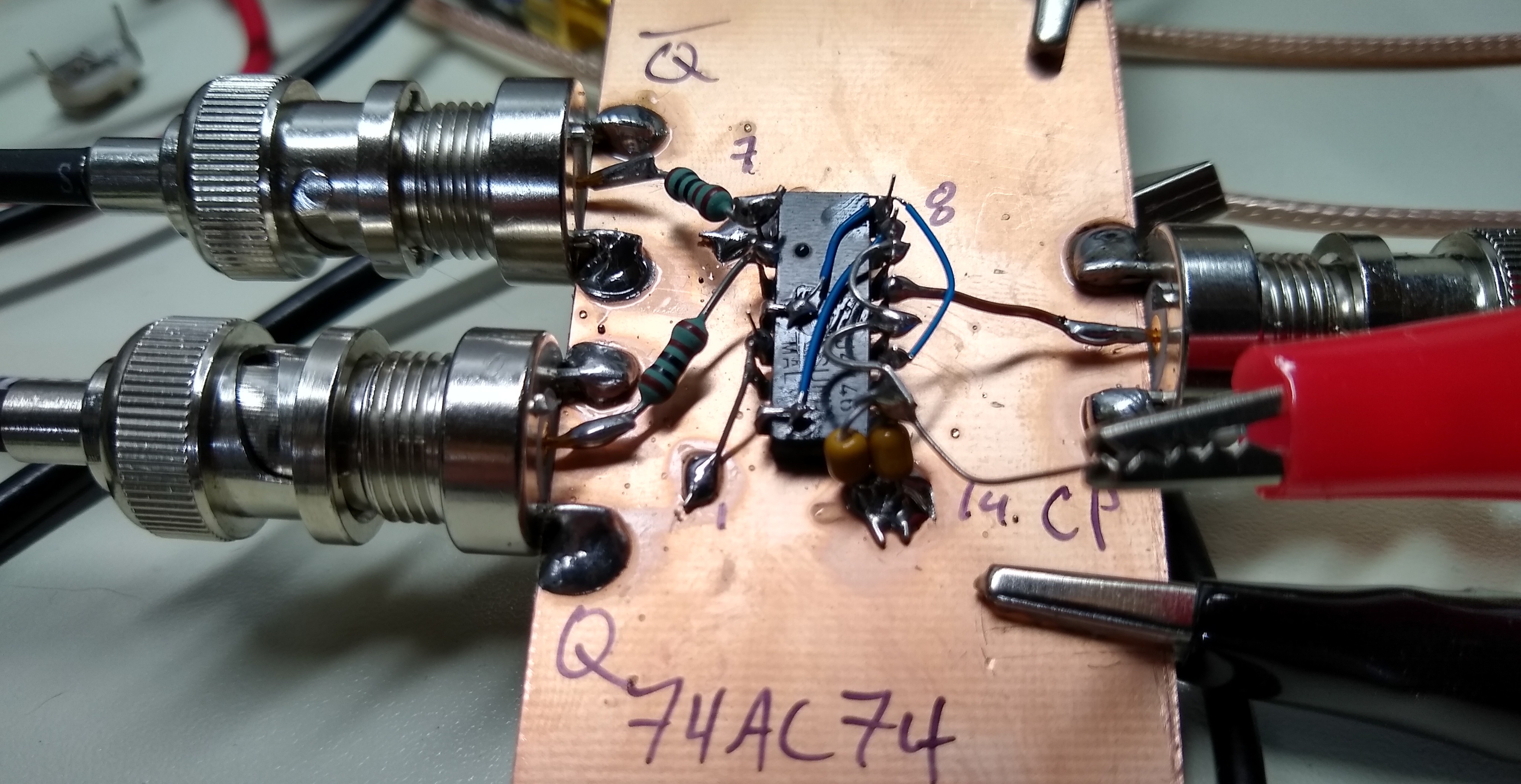
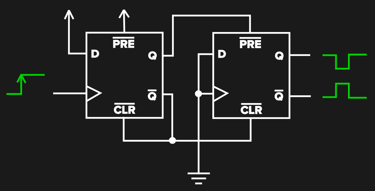
74AC74 Differential Pulse Generator
03/30/2019 at 16:05 • 0 commentsI had looked at the 74xx74 as a possible differential-output generator before, but the fact that it's a flip-flop complicates matters. I finally came up with a way to do it, though. A fairly simple circuit using one flip flop creates short (3.2 ns) pulses from each input edge.
![]()
The first flip-flop does all the work. The data line is tied high, so on the rising clock edge, the Q output goes high and Qbar goes low. Qbar is connected back to the CLRbar input, which resets the flip flop as soon as it has been set. The output from this flip flop is a differential pulse, but the Qbar output is slightly loaded. Because I had another flip-flop in the package, I added it as a kind of buffer on the outputs. The two outputs from the second flop should be more symmetrical.
![]()
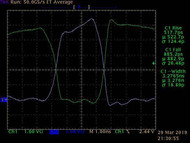
The outputs look OK for the kind of nonsense I'm trying here. One goes high and one goes low for around 3.2 ns.
![]()
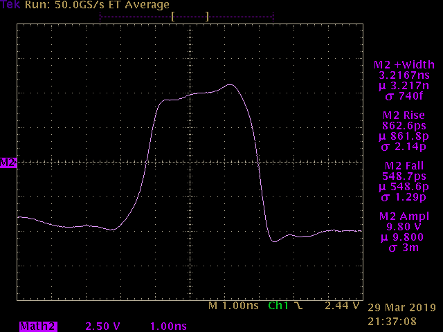
More interesting is the differential signal, estimated here by oscilloscope trace math.
![]()
The differential pulse has an amplitude of around 9.8 V (2x the 5 V supply), with a rise time of around 900 ps and a fall time around 550 ps. The width at the 50% threshold is 3.2 ns.
The pulse width probably depends on voltage and temperature, and I'd expect a lot of part-to-part variation. But if you were driving a track-and-hold sampler where only the edges matter, then this should be fine. It's not the ultimate in speed, at least with the 74AC version, but it would probably have faster edges if built with 74LVC parts. I'm going to have to try it now.
The nice thing about this solution over the 74LVC2G157 I looked at before is that it takes care of creating a relatively short pulse for you. This could simplify things a bit - at least for some sampling topologies.
If you were to use this to drive a diode sampling gate, you'd want to sample on the falling edge because it's almost twice as fast.
-
Maybe a 30 ps rise time - no way to tell (yet)
03/28/2019 at 15:06 • 0 commentsI built a fast-edged buffer using a SY88022L laser-diode driver. The datasheet claims edge rates below 25 ps (20%-80%), which should be around 30 ps if measured 10%-90%. It seems to work OK, but the problem is that my best scope (so far) only has a rise time of around 300 ps, an order of magnitude too slow. This is a design I'll clean up and officially release once I'm sure it works - people might find it useful.
![]()
The output driver has a differential CML input, so I used an ADCMP607 CML-output comparator as a buffer/translator from LVCMOS input signals. I'm not sure yet how much jitter this adds, but for just generating an edge without caring *exactly* when, it's fine so far. The ADCMP607 has built-in hysteresis you can adjust with a resistor. Looking at the image, I realize I populated that spot with a capacitor instead of a resistor. Oops. It may work even better with the parts in the right place :-)
![]()
The thing runs on a 3.3V supply, and the input threshold is set at half the supply voltage. For a quick breakout-type test of the SY88022AL, it seems to work pretty well.
There's sites on the PCB for a resistive pullup on the output to increase the voltage step, but I haven't tried doing this yet. The output has around a 1.3V amplitude into 50-ohms. Between the two differential outputs, this is a 2.6V swing. I need at least 3V to drive a diode sampling gate. I need to go back to my notes about this circuit and see if this is performing like I thought it would.
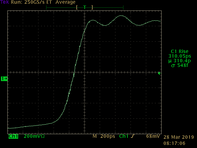
The best measurement I can get of the output shows a 310 ps rise time. Of course, this is a 1 GHz scope, so this is really just a measurement of the scope itself, equating to a bandwidth of 1.13 GHz. I have every reason to believe the edge is significantly faster than this, although I have no way to prove it yet.
![]()
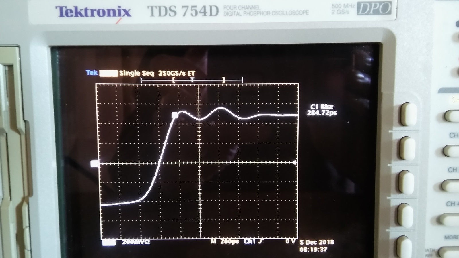
This trace looks an awful lot like the following shot that was in the ebay listing where I bought the scope. This trace was taken with one of Leo Bodnar's pulsers which achieve 40ps outputs. Note the sloping before the edge and nearly identical ringing after. That must be the scope itself. This is a very good sign, indicating that I may have achieved a good short pulse. Depending on how I set the scaling, I can get the scope to read out measurements in the 280 ps range like in the photo.
![]()
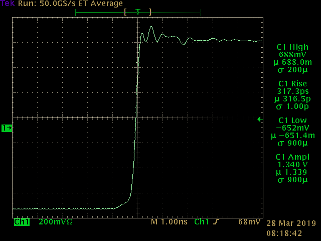
The scope's response makes everything at this scale "look" slow. Here it "looks" faster:
![]()
I really need a faster scope in order to build a faster scope. I wonder what's on ebay today.
EDIT: a friend with a 20 GHz scope has offered to measure this for me. Stay tuned.
-
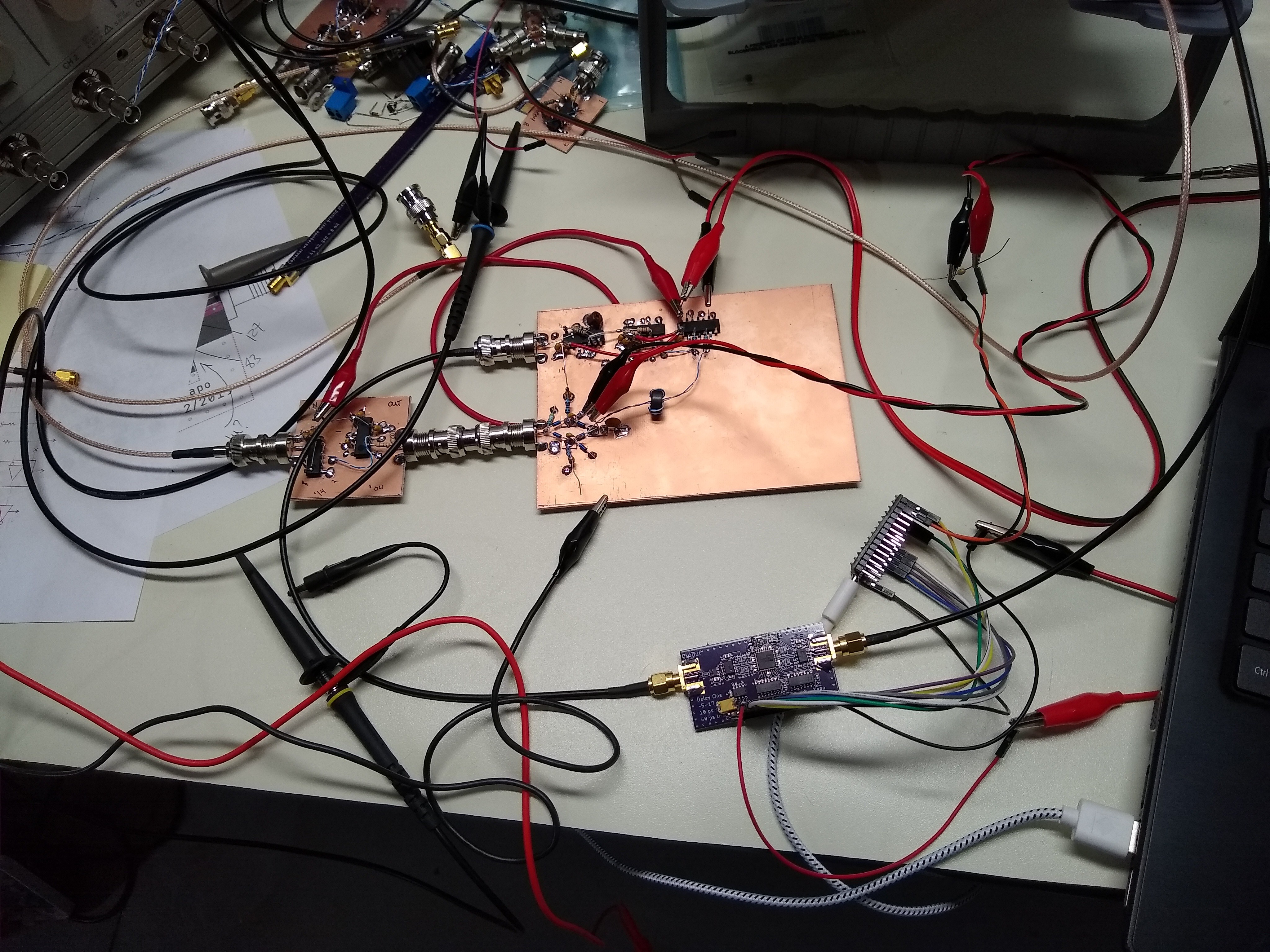
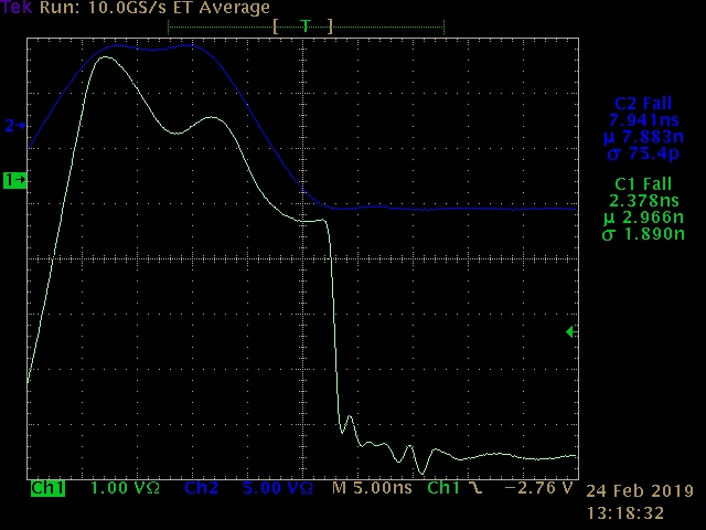
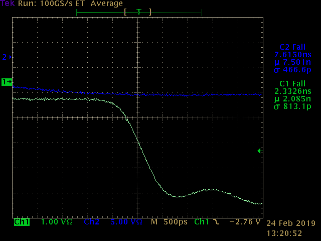
Almost an oscilloscope
03/22/2019 at 17:53 • 0 commentsI made a big mess on the bench, and got some decent data using the toy sampling head and the delay generator. Despite the look of a terrible layout, it manages 100 GS/s (equivalent time) and 180 MHz front-end bandwidth.
![]()
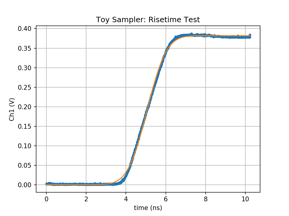
I tested the bandwidth using one of the previous edge generators that manages a modest 666 ps rise time. The resulting measurement has an approximately 1.97 ns measured rise time, which corrected for the rise time of the pulse itself is probably closer to 1.86 ns, from which we can infer a bandwidth of around 188 MHz. I estimated the rise time by least-squares fitting the best Gaussian step to the data (orange line). It's not a bad fit, really. This is probably due to all the errors summing into an approximately Gaussian response. The Central Limit Theorem saves my ass again.
![]()
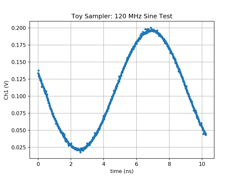
Next, I tried a sine wave. My DDS only goes up to 120 MHz, which looks a little big on this timescale, but still recognizable. The individual samples are around 10 ps apart, although I didn't calibrate the timebase. That's 100 GS/s. Not bad for less than $20 in parts (single quantities).
![]()
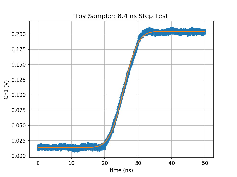
As a final test, I looked at the output of my DDS set to the fastest edge it can produce, spec'ed at 8.4 ns. To get this trace, I stitched together five separate captures of 10 ns each.
![]()
The DDS says the step has an 8.4 ns rise time, but I haven't verified this with a "real" scope. I'll do that next time I'm in the lab. The Gaussian fit works well again on this step, estimating a 8.59 ns rise time. I'll write up how to fit a Gaussian step and estimate rise time from it at some point in the near future.
You can see more noise in these samples, because I used a tighter sampling loop that doesn't let the storage capacitor settle as long. There's a log upcoming about the details.
I'm also not sure how to automatically extend the sweep time like in this example. So far, it's been some trickery involving the DDS, but I really need a general solution. I can cascade the SY89296U programmable delay to give increments of 10.24 ns, but at around $10 each, it would be an expensive way to reach microsecond-length sweeps.
More research is required. And large government grants.
-
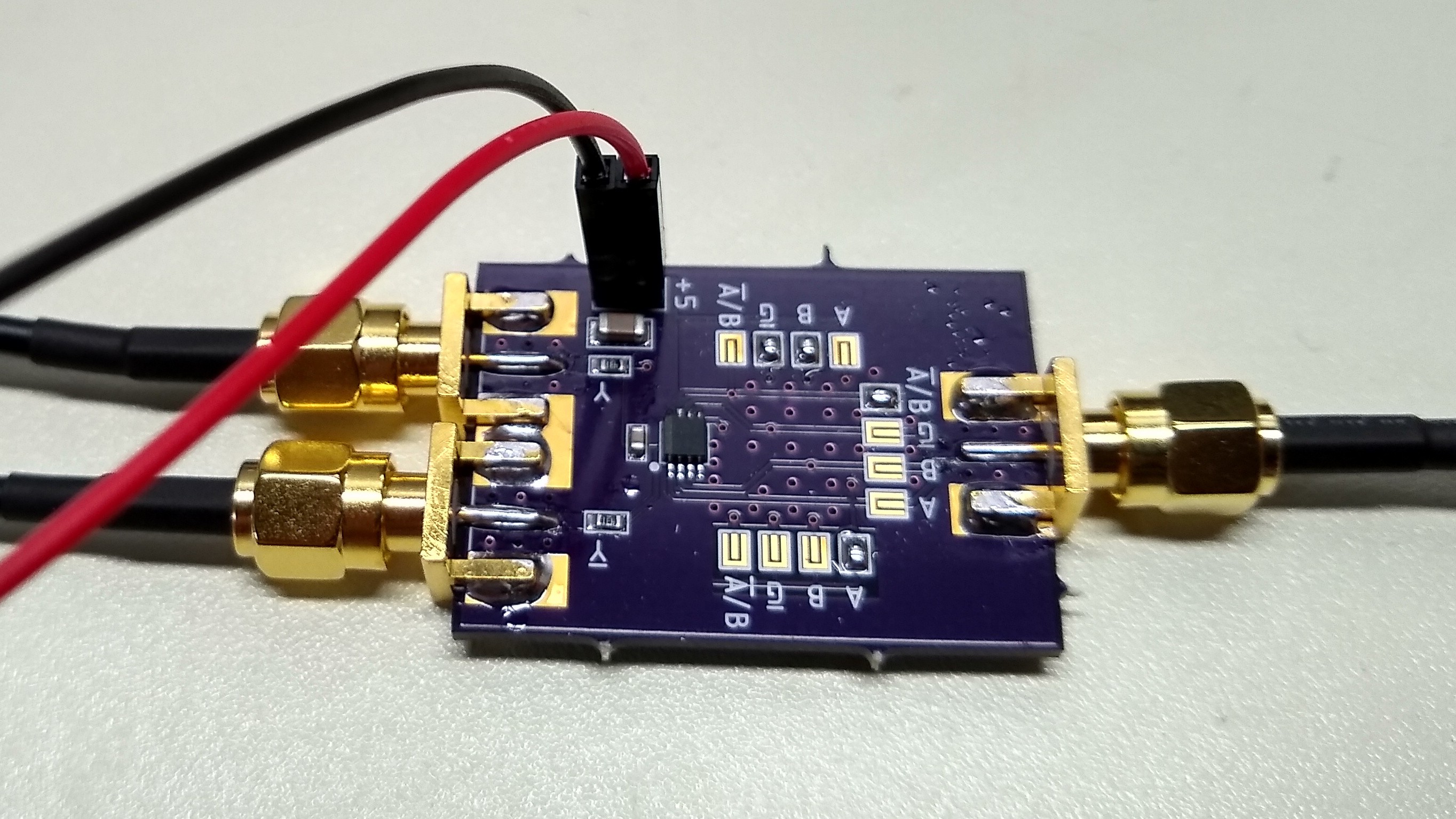
There is a differential-output CMOS logic gate, after all
03/22/2019 at 15:39 • 2 commentsUntil now, I believed that such a gate was the stuff of myth, like rainbow-farting unicorns. Now that I've finally found the 74LVC2G157, I'm going to take a little closer look at every horse I see, just in case.
![]()
So, here's the deal: the Y and Ybar outputs of the 74LVC2G157 2:1 multiplexer are as close to a differential output as you can find. I had previously measured the Q and Qbar outputs of a 74AC74 flip-flop and found them to have pretty low skew, but the fact that it's a flip-flop makes it a little difficult to use as an output buffer. The 74LVC2G157 seems even better, plus being 74LVC logic, has rise and fall times around 500 ps or so.
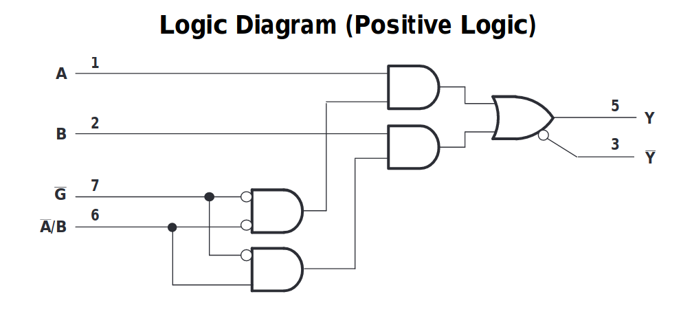
I designed a lavish breakout PCB to test this part mostly because I didn't feel like soldering the tiny SSOP pins by hand. The board has solder bridge footprints to allow any of the inputs to be connect to ground, +V, or the input signal. It turns out I only needed to test one combination. The logic of the mux is straightforward: Abar/B selects one or the other input to be routed to the output, when the Gbar input is low. The output is provided as Y and Ybar, which can be abused as a differential pair for all sorts of nefarious purposes. This is my kind of part!
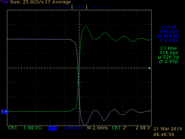
![]()
By tying the A input low and B input high, the output follows the Abar/B input, producing a differential-output buffer. The output looks really good on the scope: the outputs transition in around 500 ps, and cross at about 1/2 the supply voltage, indicating a relatively low skew. I didn't measure the skew between the outputs directly, but it looks small enough to be useful. I'm not sure where the ringing is coming from; the outputs are probed with 10:1 resistive Z0 probes which should be fine at these speeds. It may be cheap RG174 cables from ebay - I'll have to re-test with some decent RG316 ones I have around somewhere. At least the ringing is relatively symmetrical and balanced.
![]()
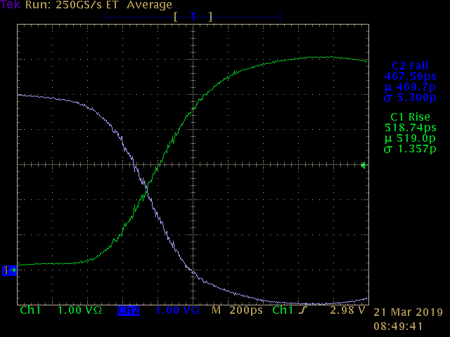
Zooming in a bit, we get a better look at the transitions:
![]()
The traces don't cross exactly at 1/2 the supply voltage, indicating some possible skew, but it's relatively small. This could also be due to some other factors: I didn't check the two oscilloscope channels for perfect alignment, for instance. In any case, this is good enough to do some further work with. It's certainly better than tuning a couple of XOR gates.
Just to put this into perspective, this part is generating a 10 V differential step in half a nanosecond (it could be pushed to 11 V and still be within the recommended range according to the datasheet). This is plenty good enough to create a sampling pulse for an sampling oscilloscope of several GHz, since the diodes will switch on a much shorter segment of the transition. There was an old design for a sampling scope in Electronic Design (nearly 20 years ago now!) that achieved 1 GHz bandwidth with 2.2 ns transitions from the output of a comparator. This transition is nearly 5x faster. That's pretty exciting.
I also have some breakout PCBs for laser diode drivers with 25 ps transitions being fabbed at the moment, but this CMOS multiplexer might enable some incredibly-dirt cheap applications, like maybe a standalone (no oscilloscope required) TDR with spatial resolution in the cm range.
EDIT:
You know, in the rush I designed this PCB, I didn't check that the traces on the PCB are exactly the same length. There probably isn't much difference, but it could be a contributing factor.
-
A Real Step Recovery Diode: MA144769
03/01/2019 at 17:01 • 2 commentsI found some actual step-recovery diodes at Mouser. They're not the fastest ones available, with only a 150 ps maximum transition time, but that's still pretty good. They're available in SOT-23 and SC-79 packages, so I bought a few in each. I was able to test one today with the same setup I had used to test a 1N914 earlier.
![]()
Here's the input pulse (blue) vs the output (green). The diode has sharpened the fall time considerably, from 7.8 ns to 362 ps according to the scope auto-measurements at this time-scale. It's actually much faster than that.
The circuit to test this diode is the same one I used before:
![]()
In this case, the diode was in a SOT-23 package, so I used a little adapter PCB to mount it to two BNC connectors.
![]()
Here's the falling edge of that pulse again, at 200 ps/div. The scope now says it has a 278 ps fall time, but guess what? That's the fall-time of the scope itself! The diode probably has a fall time under the 150 ps maximum spec on the datasheet. I'll just have to find some clever way to verify it.
![]()
This seems promising. These diodes are only around $2 each, and are easily fast enough to generate strobe pulses for a 1 GHz sampling head.
I'm thinking I can drive one of these SRDs with a commercial MOSFET driver IC. The driver doesn't need to be particularly fast (a few ns transitions are fine), but needs to handle some hefty currents and have low jitter.
-
I Finally Made My ECL Bones
03/01/2019 at 04:15 • 1 commentI got the delay line working tonight. It took a a little re-work on the PCB because I didn't understand the SY89296 datasheet. Luckily it was just one of the control lines and not the data, which is high-speed and impedance controlled and doesn't like to travel in blue wires very much.
![]()
I learned two important things. First, PECL is crazy power-hungry. I "debugged" the board for an hour looking for shorts or reversed components after noticing it drew 300 mA when I first applied power. I come from CMOS land, and expected an order of magnitude less current. Of course, once I dug through all the datasheets, I realized this was normal. The PCB is nice and toasty.
Second important thing: you have to use a *light* touch cutting traces on 4-layer PCBs. That second layer (in this case a ground plane) is only 6.7 mils under the top layer. It's very easy to cut down into the next layer and possibly short stuff. I'm used to hacking away willy-nilly with a knife, and that just doesn't cut it in this case (pun intended).
Anyway, I got the thing working. There's a 10-bit digital control and a 12-bit analog fine tuning of the delay. I measured approximately 9.54 ps per digital step, and around 28 fs per analog step, although individual steps of both both were lost in the jitter noise of the delay and the measurement on the scope I was using. Individual steps of the analog tuning will never be of much use - the intention is to simply use the analog tuning voltage to get the digital steps in nice 10 ps increments, although I'll certainly see how far I can push things.
The next step is to build a feedback oscillator with this delay line, and measure the oscillation frequency accurately to calibrate the delay.
Maybe I'll make a quick oscilloscope with it first just to see it work.
-
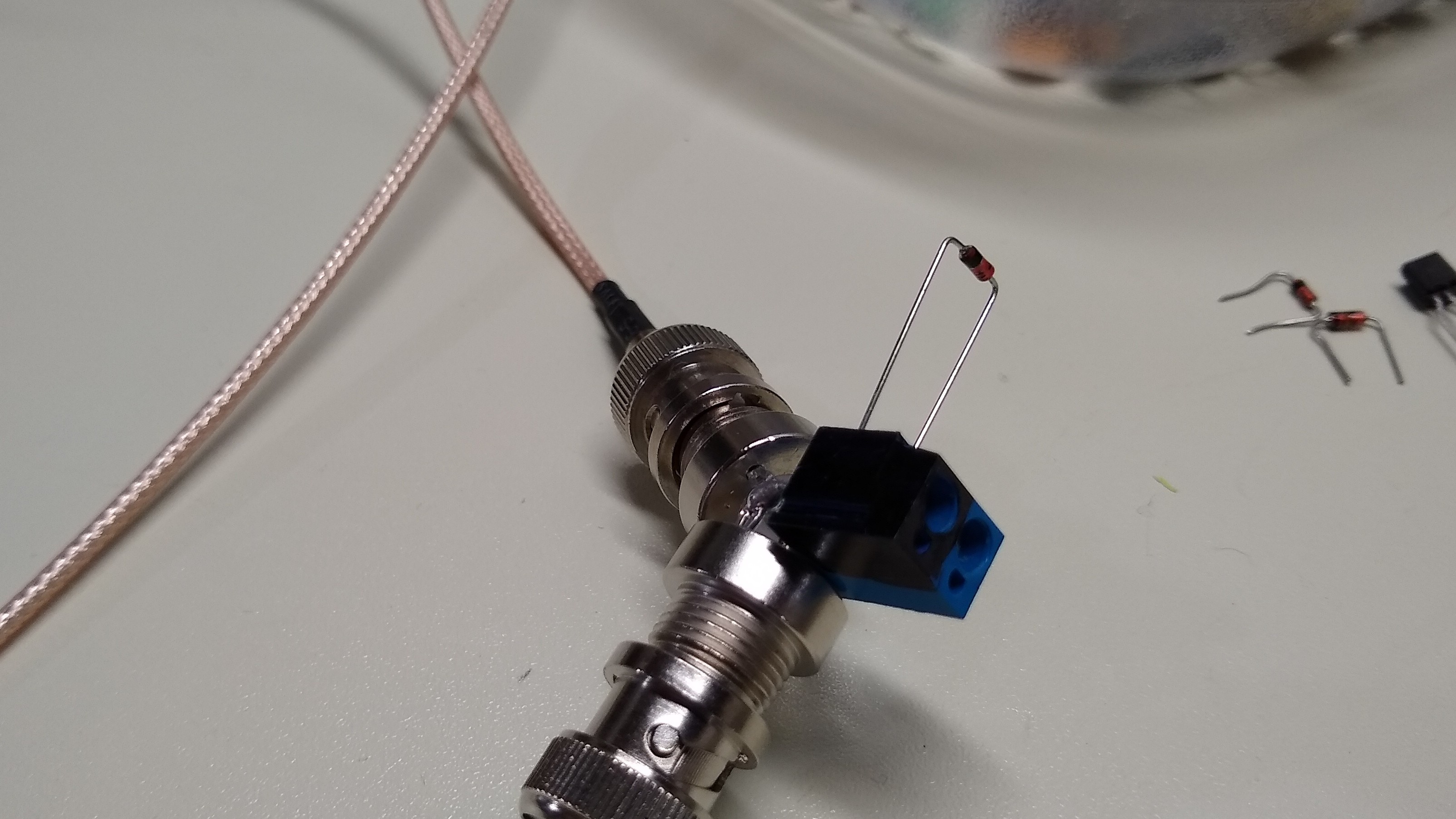
My First Step Recovery Diode: The Lowly 1N914
02/25/2019 at 13:13 • 0 commentsThe sampling strobe generation work is taking some strange twists (details to come), but one branch I'm exploring is solidly traditional: step recovery diodes (SRDs). I have some real ones on order (not quite as unobtainium as I thought), but in the mean time, it turns out that the bog-standard 1N914/1N4148 type diodes can function as decent, if slow, SRDs.
![]()
In case you're wondering, those long leads are there for a reason (see below). There's not much to the test circuit - the diode is just shunted across the output of a pulse generator and measured with an oscilloscope.
![]()
Here's the measured output from the diode. Channel 2 (blue) is a copy of the output of the pulse generator (from another output channel) for reference. During the positive swing of the pulse, current flows through the diode. When the input polarity is reversed, the diode continues to conduct for a brief time, then suddenly "snaps off." You can clearly see the rapid drop in conduction, with the waveform becoming almost vertical at this scale.![]()
Zooming in, we see that the rapid drop has a fall time of around 800 ps (ignore the automated measurement, it's looking at the overall drop from the top of the pulse). The pulse generator has a fall time of around 8.5 ns (compare the blue trace), so the diode has sharpened the fall time considerably.
This diode is very slow compared to diodes designed as SRDs, but it illustrates the concept.
![]()
Those long leads? They add some inductance which peaks the pulse a little. Here's the same diode with short leads. Note how the bottom edge of the pulse droops a little. In this regime, the inductance of a few cm of wire matters, and sometimes can be used to advantage. Of course, I found this by accident :-)
![]()
There is a paper out there on the internet somewhere that used a 1N4148 diode like this to produce a strobe for a moderate-speed sampling gate. Now I can't find it again, and it doesn't appear to be in my collection of papers. When it turns up again, I'll post the link here.
-
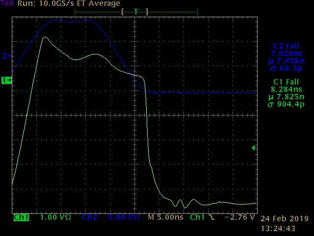
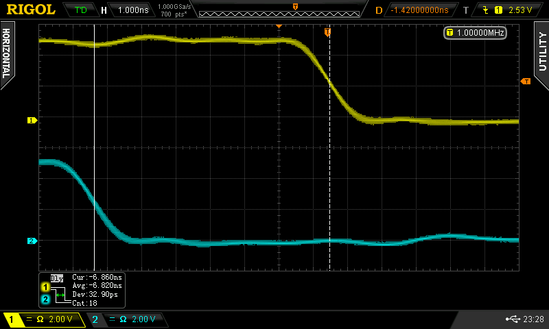
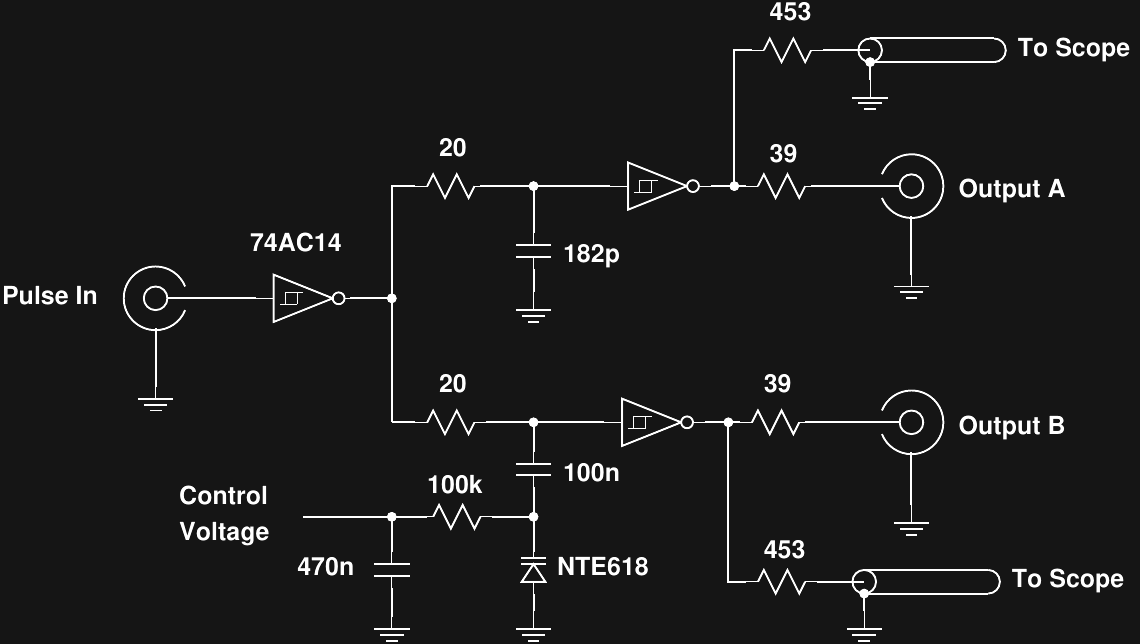
The Old Delay Generator
02/11/2019 at 02:58 • 0 commentsThis is what I've been using so far, and will be until the new PCBs come back. It's a little primitive, and not entirely stable, but it allows adjustable delays with a resolution of tens of picoseconds. It's also really interesting to see how ground bounce and supply sag influence the high and low voltages of the "other" channel with these two output drivers in the same package.
![]()
The circuit has a pulse input and two outputs. You can tune the timing of one output relative to the other with a control voltage. The whole thing is breadboarded ugly/dead bug style on some copper clad. There's plenty of room for other stuff :-)
![]()
The circuit isn't very complicated. An NTE-618 varactor diode is used in an RC delay circuit to move the edge of one output relative to the other. The stationary edge uses a similar RC circuit with a fixed capacitor to place it approximately in the middle of the range of the variable output. You can tune the output over about 10 ns, and a 20-turn potentiometer allows setting the delay with a resolution below 50 ps.
![]()
The control voltage is non-linear and uncalibrated, so I tapped the outputs and monitor them on a 300 MHz scope to determine the relative time between the edges. The modern Rigol scope has better statistics on this kind of measurement than my ancient 1 GHz Tektronix, so I used it. Due to the large levels of jitter in the system, you have to average 20-50 measurements to get a stable result. This isn't as limiting as you might think, since you can use MHz repetition rates.
Calibration
I had intended to retire this circuit and wait for the fancy new PCB to arrive, but after a brilliant observation by @salec on the last log, I think I'll do a few more experiments with it. The awesome idea was to calibrate delay generators by connecting them as feedback oscillators and measuring the resulting frequency. This frequency is related to the inverse of the delay time and frequencies are easily measured to parts-per-million accuracy.
I think I'll wire up a 12-bit DAC and op amp on the PCB to allow driving the varactor with 0-12V, hook up some kind of oscillator circuit, then try to calibrate the delay vs voltage. It's too bad my bench frequency counter doesn't have a PC connection. I might be able to use the spectrum analyzer, although it would take a bit of coding. Actually, it might be easiest just to find one of the OCXOs, TCXOs, or rubidium oscillators I have tucked away and throw together a quick frequency counter on an FPGA.
-
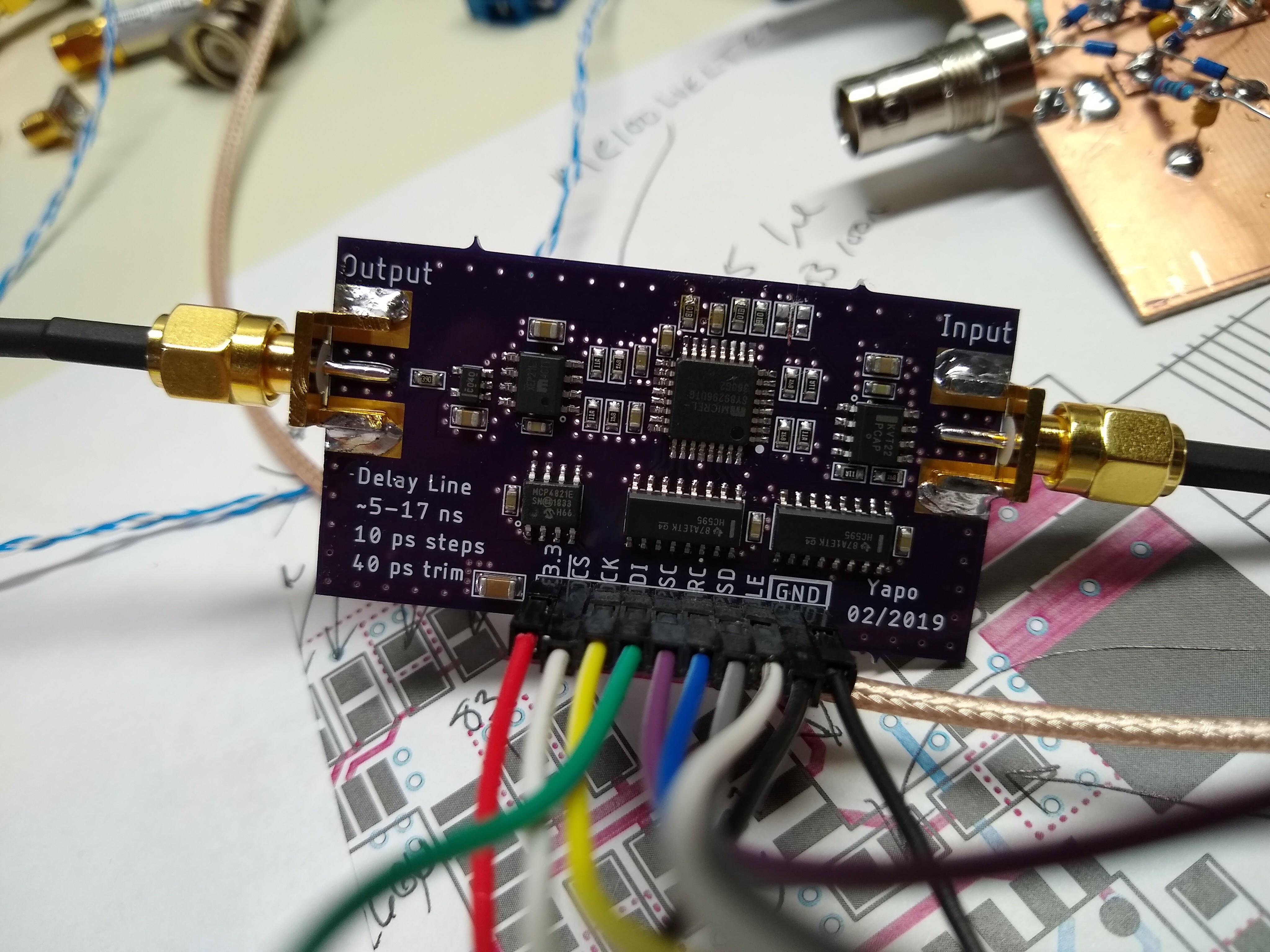
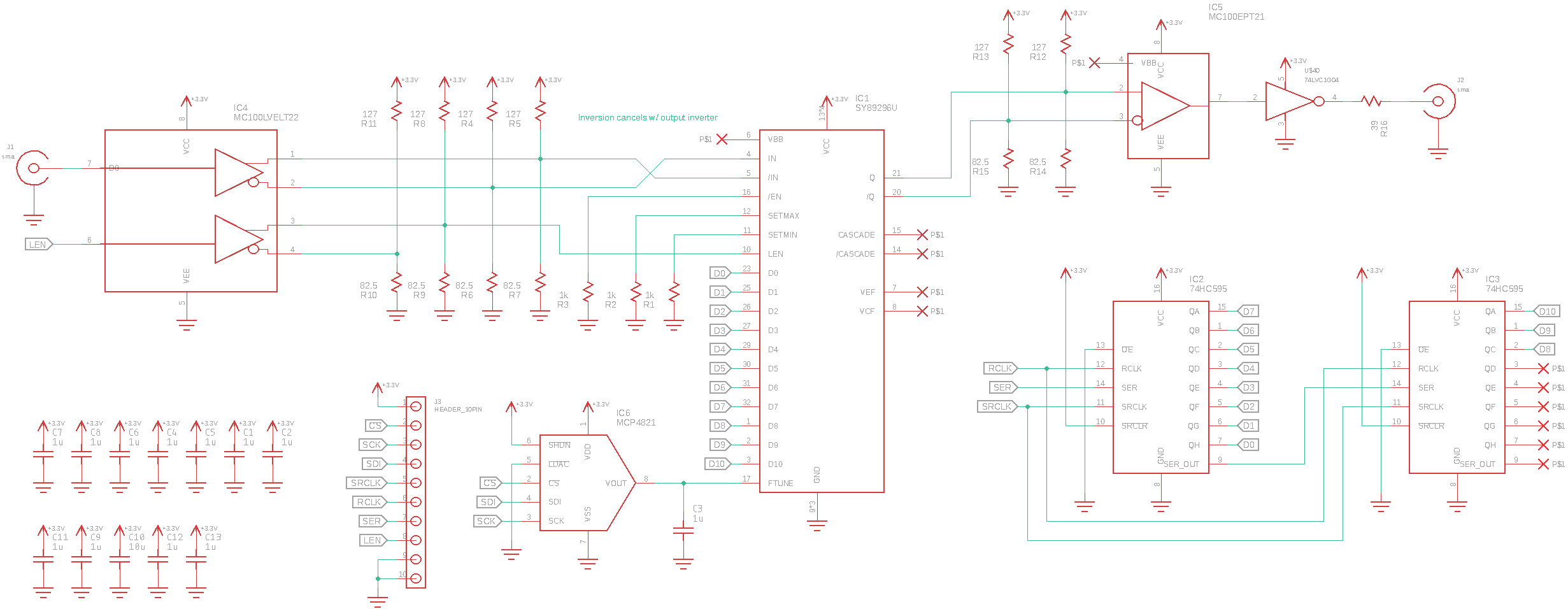
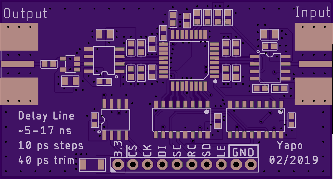
Adjustable Delay with 20 Femtosecond Resolution
02/09/2019 at 17:05 • 10 commentsOf course, jitter will be around three orders of magnitude larger, but it remains to be seen what accuracy can be obtained by averaging many measurements. Wait, I'm getting ahead of myself. This PCB is a digitally-adjustable delay line built around an SY89296U programmable delay IC. This part, designed for adjusting clock edge timing, has a 1024-step digital delay control with 10 ps resolution, plus a 40 ps analog trim voltage input. I drive the trim voltage with a 12-bit DAC, allowing a theoretical delay step size of 20 fs. There will be non-linearities and jitter which limit the usable resolution to much greater step sizes.
![]()
The board has two 74HC595 shift registers to hold the 10-bit delay control word, plus a MCP4821 12-bit DAC for generating the fine-tuning voltage. Since the delay IC uses LVPECL signalling, LVCMOS translators are used on the input and output. This is really nothing more than a breakout for the SY89296U.
Resolution
The SY89296U has 1024 nominal 10 ps digital delay steps, with less than 10 ps total jitter (2 ps cycle-to-cycle). It additionally has an analog fine-tuning voltage input with a resolution of 40 ps/V. I drive this input with a 12-bit converter with 0.5 mV step sizes, allowing for a minimum step size of 20 fs. This 20 fs number is somewhat meaningless, since it will be swamped by other issues.
Jitter
The SY89296U has a maximum 10 ps total jitter. One of the translators has 5 ps, the other has 2 ps. I don't know about the 74LVC04 inverter at the end; I suspect it has around the same. I might be looking at 15-20 ps total jitter through the whole chain. That's not too bad, and the results can be improved by averaging over many measurements.
Accuracy
The accuracy of the generated delays depends not only on the resolution and jitter, but the calibration of the SY89296U. The actual delays generated can vary by about 20%, according the the datasheet. So, I need a way to calibrate the delays. So far, the best answer I have is another PCB I just sent out which has dual TDC7200 time-to-digital converters. This should be able to measure delays with 55 ps resolution and 35 ps standard deviation; it's possible I can achieve better results by averaging over many samples, but I'm not sure how far I can push it.
I'm also wondering about other ways to calibrate the delays. Any suggestions?
I think I need to dive into the literature at this point.
The PCB
This was a new one for me. The LVPECL parts require special care and feeding, with their impedance-controlled and terminated differential traces and being referenced to Vcc instead of GND. I went with a 4-layer PCB, obviously. I don't mind paying extra for the 4-layer job at OSH park, I just wish there was a super-speedy option for this stackup.
![]()
Hey everyone, order more 4-layer PCBs, so they'll do one.
This PCB has been ordered as of 2019-02-09.
I don't think I've ever used the word femtosecond before. It's kinda fun.
The Rise and Fall of Pulses
A project in which I try to go faster and faster