 Trevor Johansen Aase
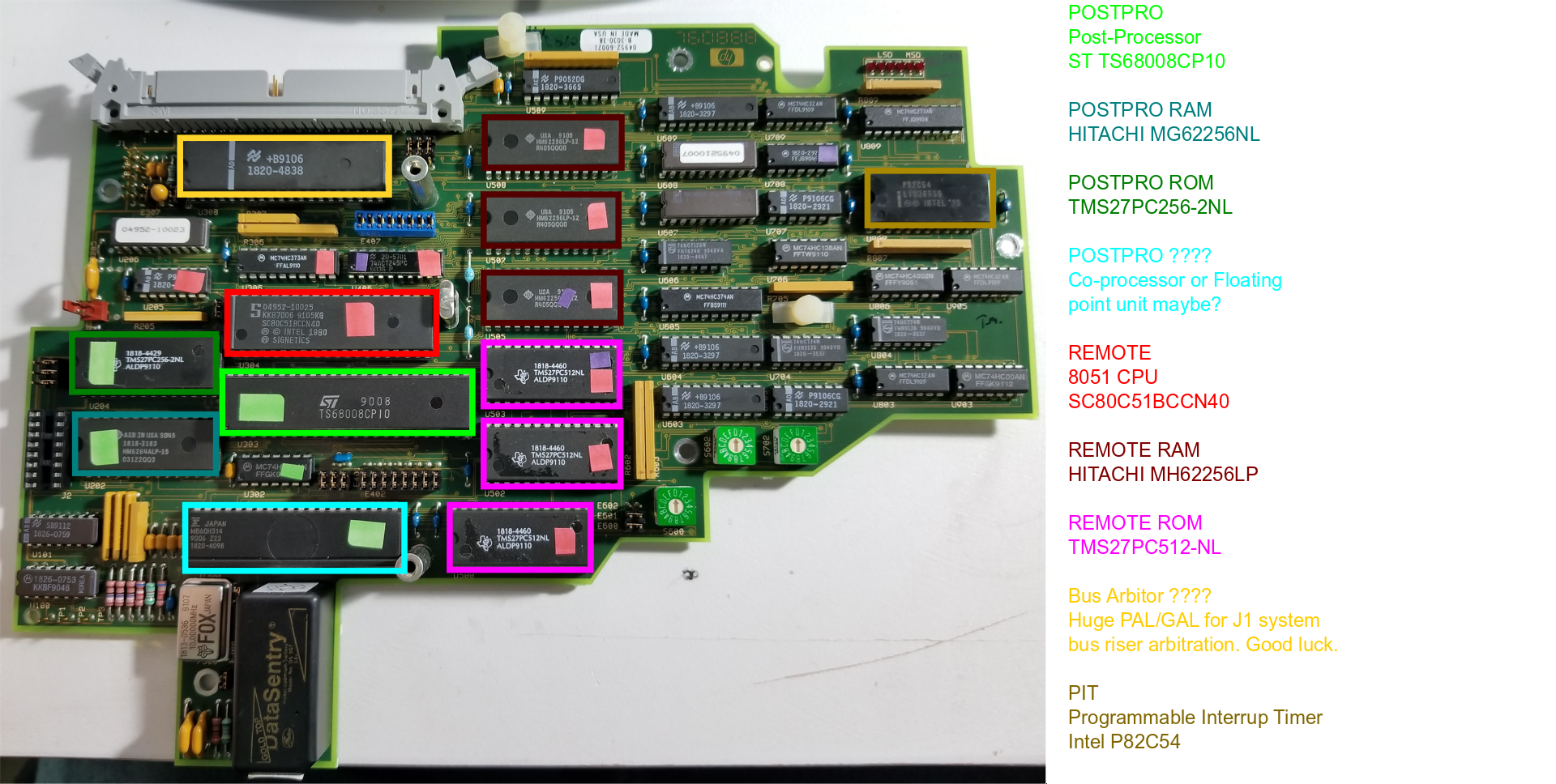
** Very Confused Point **
I have removed the PIO, Zilinx z80, Toshiba z80, toshibas ROM, Postprocessor CPU/RAM/coprocessor, the 8051 AND the disk board is not plugged in. THERE ARE NO MORE PROCESSORS IN THIS THING. WHY DOES IT STILL WORK?!
All the self test fail of course but the hardware tests run an the main menu runs, I can setup the pods menus (nothing actually works of course) but how does the menu system work if there is no processor to handle the keyboard requests?!
I am starting to think the giant PAL/GAL is actually a complete custom CPU. As it shares access to the ROM's I would guess its 8051 based. Once the roms are dumped and I find system code it should be obvious if its 8051 or z80.
** Very Confused Point **
This is a very complex board and is at least 4 layers. I didn't expect any multi layer board for a piece of equipment all through hole and from the mid 80's. This would have been a heck of an expensive board to manufacture.
Post-Processor:
We have a ST TS86008 processor with 32k RAM & ROM as well as a custom Hitachi something. The Hitachi chip has only A0..A4 attached so it must be some sort of floating point co-processor or something.
Remote:
When I pop the 8051 out of its socket the self test shows "REMOTE" failure. In the 4951C drawings remote and pod are used interchangeably it seems. If this is indeed to pods processor then the z80 and PIO on the mainboard must just be a serializer. This 8051 must do all the protocol decoding from the raw stream.
RAM & ROM:
This is definitely connected to the 8051 as well as the large GAL in front of the J1 system bus. When I pull ROM 3 the self tests and hardware test interface works but the main system does not load. ROM 3 & 2 and only the self test loads. ROM 3, 2 & 1 and nothing displays on screen. These are 64k ROM's which is also strange as most of the system can only address 64k so each ROM having distinct bits of the system is strange. I will dump them and see what's up.
PIT:
The manual shows the 4951C had a programmable interrupt generator and timer IC. As this is buried in a sea of PAL/GAL's there is no way to know what its actually attached to.
Giant PAL/GAL:
This beast is connected to all the J1 system bus address and data pins as well as the RAM & ROM chips. I would guess its some sort of bus arbiter to act as a kind of DMA between all the system CPU's and the main memory?
Discussions
Become a Hackaday.io Member
Create an account to leave a comment. Already have an account? Log In.