 morgan
As the description say.. why the heck not etch a bunch of Pyralux?
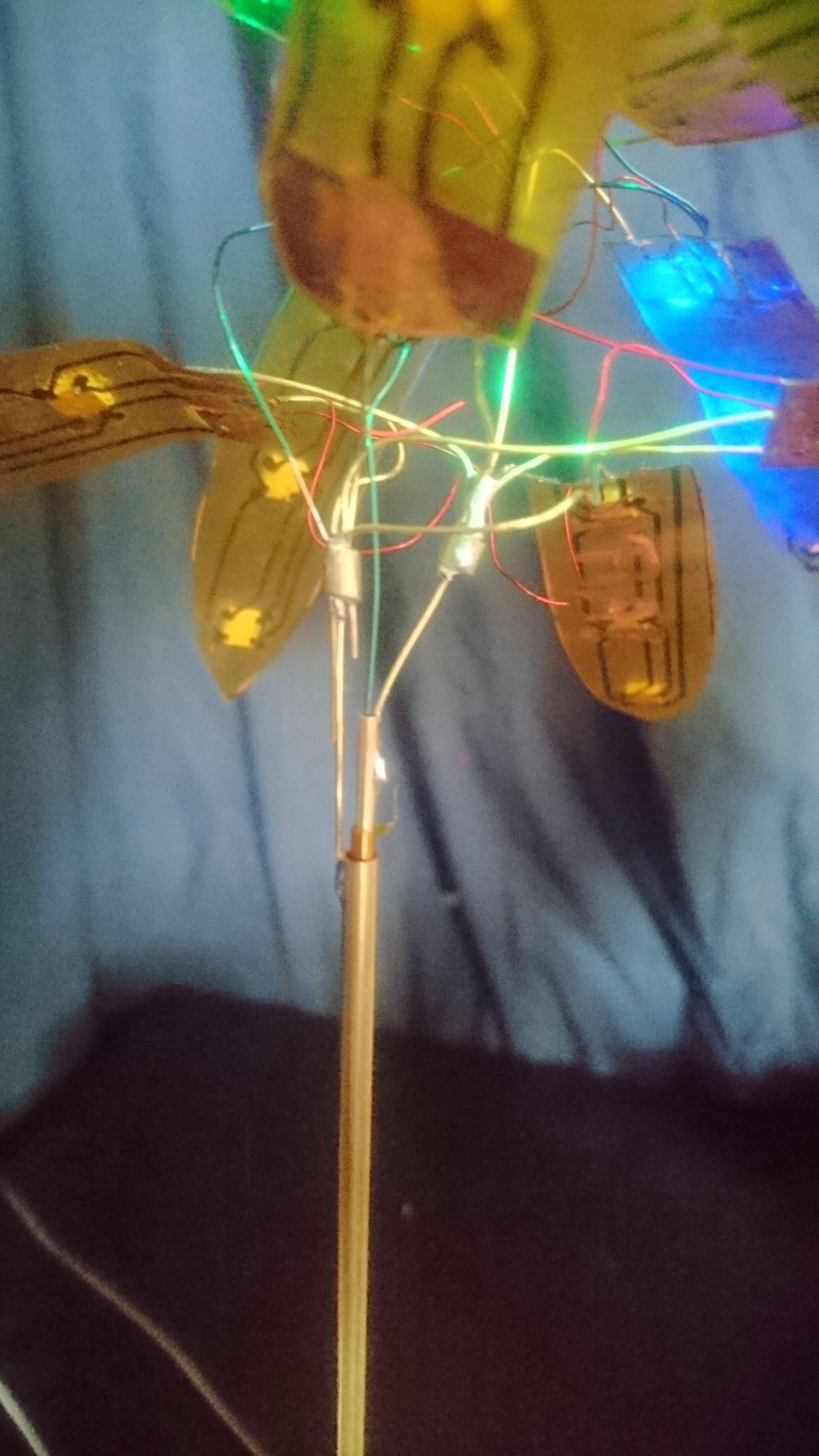
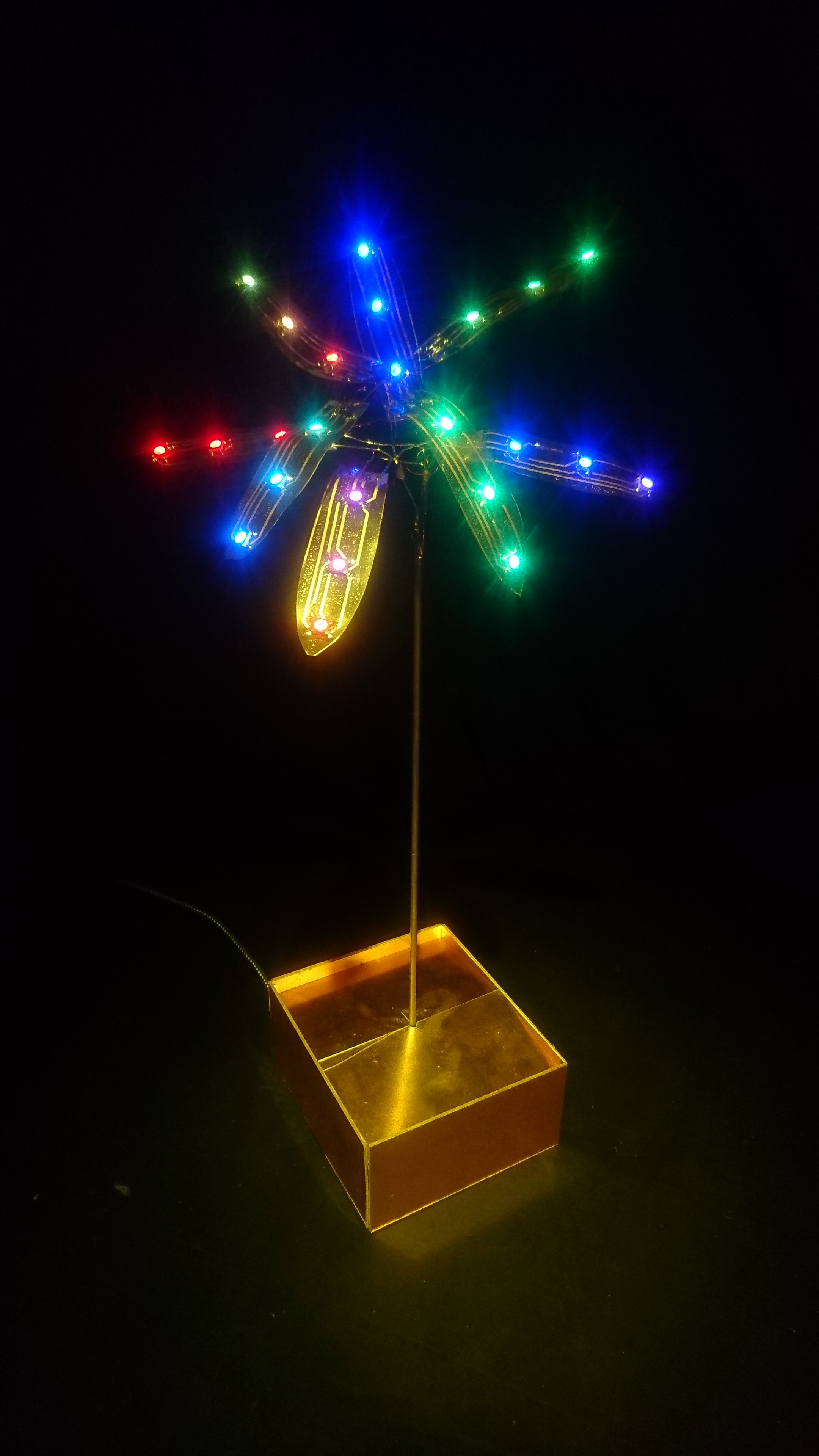
The whole project took about 8 days, almost entirely spend etching Pyrlux to make "petals". The initial vision in my head was this being more of a flower.
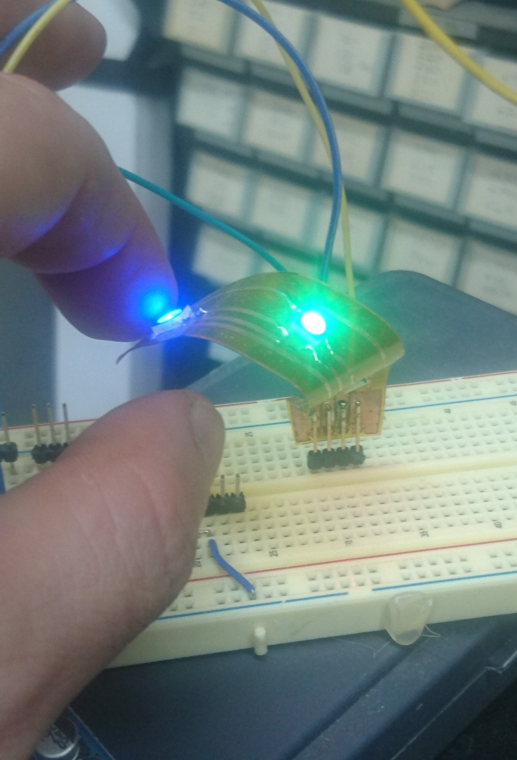
My first attempt was using APA102-2020 LEDs. This didn't work out as I was unsure I'd be able to pull off double sided routing. Things where also quite cramped with such a small outline.

This led me to start thinking about the reel of WS2812Bs I have... In light of not wanted to end up banging my head on the wall in frustration (like using this editor right now....) the decision was made to scale everything up. Larger outline, easier to solder LED.

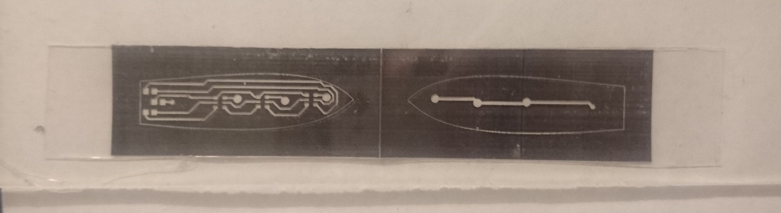 After I plot my copper layers and board outline I do some post-processing in Inkscape. The idea is to duplicate the outline and lay they front and back copper on each. Flip the back side and position across a fold line. This can then be cut and realigned. Later versions had better alignment targets.
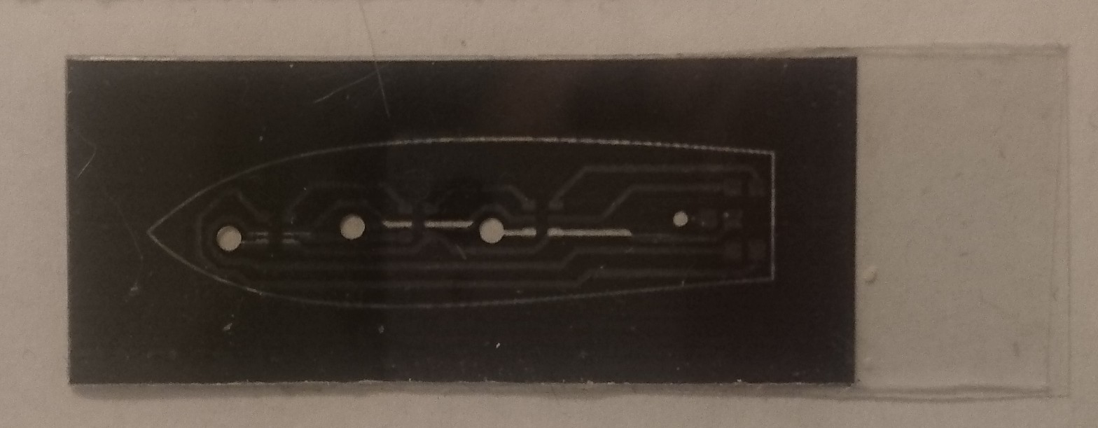
After being folded over the alignment of the front and back sides can be seen.
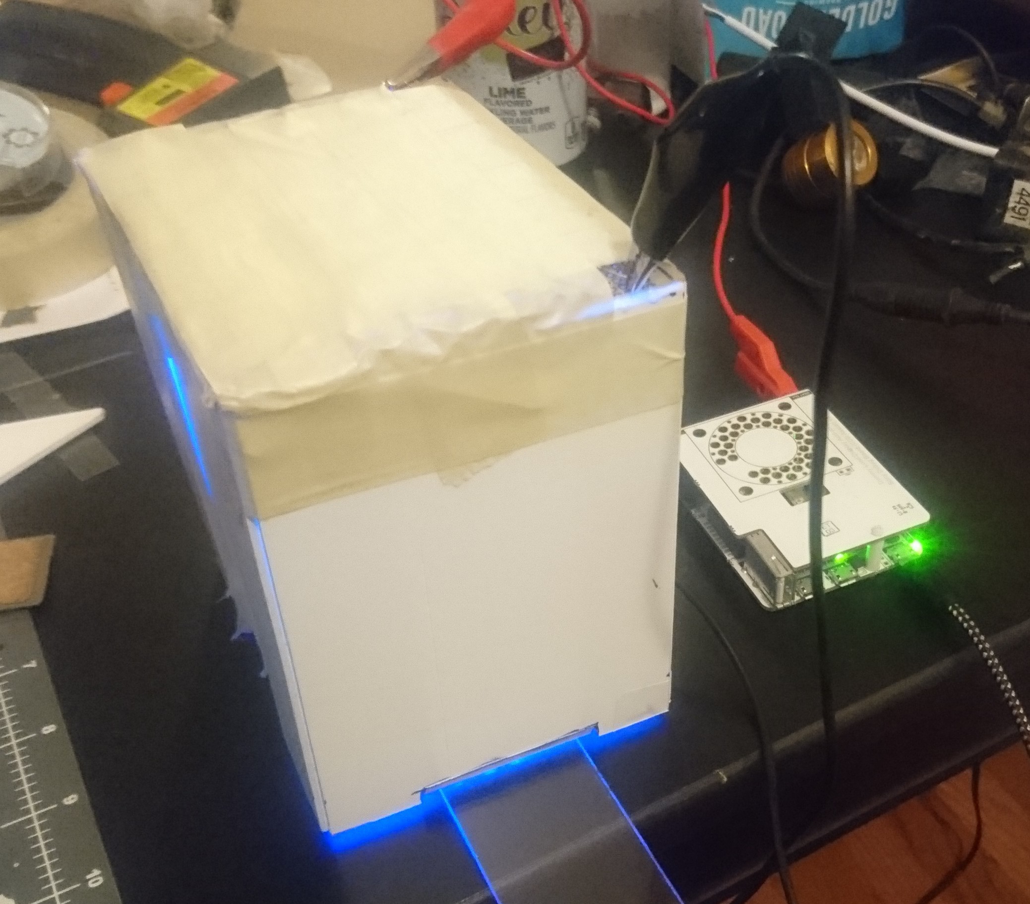
My exposure unit consists of about 60 UV LEDs run at 4V around 200mA. This was more randomly selected than anything else. 3.5 minutes yielded pretty good results. If I could get my masks darker that would go a long way. Doubling up the transparencies works pretty well for now.
For such fine detail the baords developed surprisingly well but in the end things were just too cramped. The traces at the top where too close and I was unsure if I'd even be able to solder the APA102 hence scaling up.
ACID BAAAAATTTTHHHH!!!!
I stared the process with vinegar, hydrogen peroxide and salt. It worked quite a bit better then I thought it would but had a tendency to stall and/or take so long the photo mask would start lifting. I ended up switching to mureatic acid and hydrogen peroxide with much better results. It would slow down after a while but never stalled. I found right around 54C was the sweet spot for my mixture of about 2 parts peroxide to one part HCL. I used a very small amount of salt (NaCL) also but tried to keep that to a minimum.
First Success!
After a couple of tried I started getting the process down. My photoresist seemed to be going on well (that would change), the exposure process was going very smooth and despite the vinegar method being inconsistent and slow, the first couple in the bath would turn out well. I think I got 3 good ones out of 6 or 7 the first night. I thought switching to HCL would fix this bad yield rate but the next night I was having a terrible time applying the photo resist.
Wanting to fix prior inconsistencies with how the sheets were laying down I tried the water application method. You fill a tub large enough to fit your copper with water and dunk the board then apply the firm under the water. It's really forgiving because if you have a wrinkle or anything you can just pull it back up and move it. I then would take it out and iron it at low temp. Exposures went really well but I then could not get the protective film off, the photoresist gel was gooey and sticky. It appears letting them sit over night fixes this but I need to test it more. Next time I apply film I also want to do it with de-ionized water because I got was looks like water marks.
The next couple of nights where spent tweaking and etching and not sleeping a lot for astoundingly low yields. Probably less than 50% in the end. But hey, I learned a lot and apparently my time isn't worth anything to me. I had a rough idea of how I was going to assemble them. It wasn't what I'd originally planned where I'd also etch a center "hub" to connect them but with hiccups in the etching this plan was... streamlined.
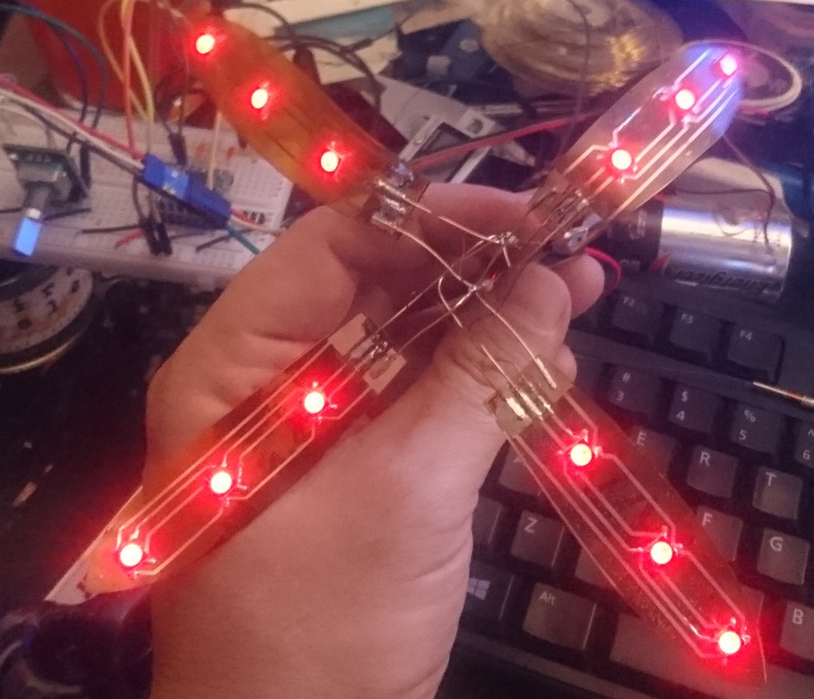
In what now feels like a nightmare that would accompany a severe case of cabin fever and Imagined connecting the petal with brass wire. The pin placement wasn't ideal as it was designed with the central PCB in mind so the wiring was quite contorted but to my surprise the first row went together quite easily. And so did the next and connecting them together!
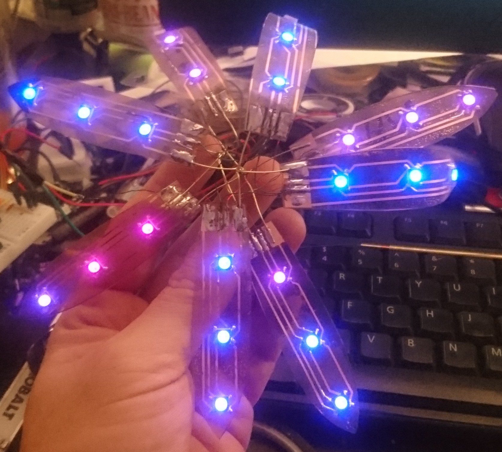
It's a palm tree! How'd that happen? Stop being a palm tree, I was making a flower. Hrmm. Well. I hadn't really figure out the rest of this yet. There were some vague ideas in my head, I'd been keeping my eye out for this 'certain vase I know I've seen before, you know, that one.' which I never found.
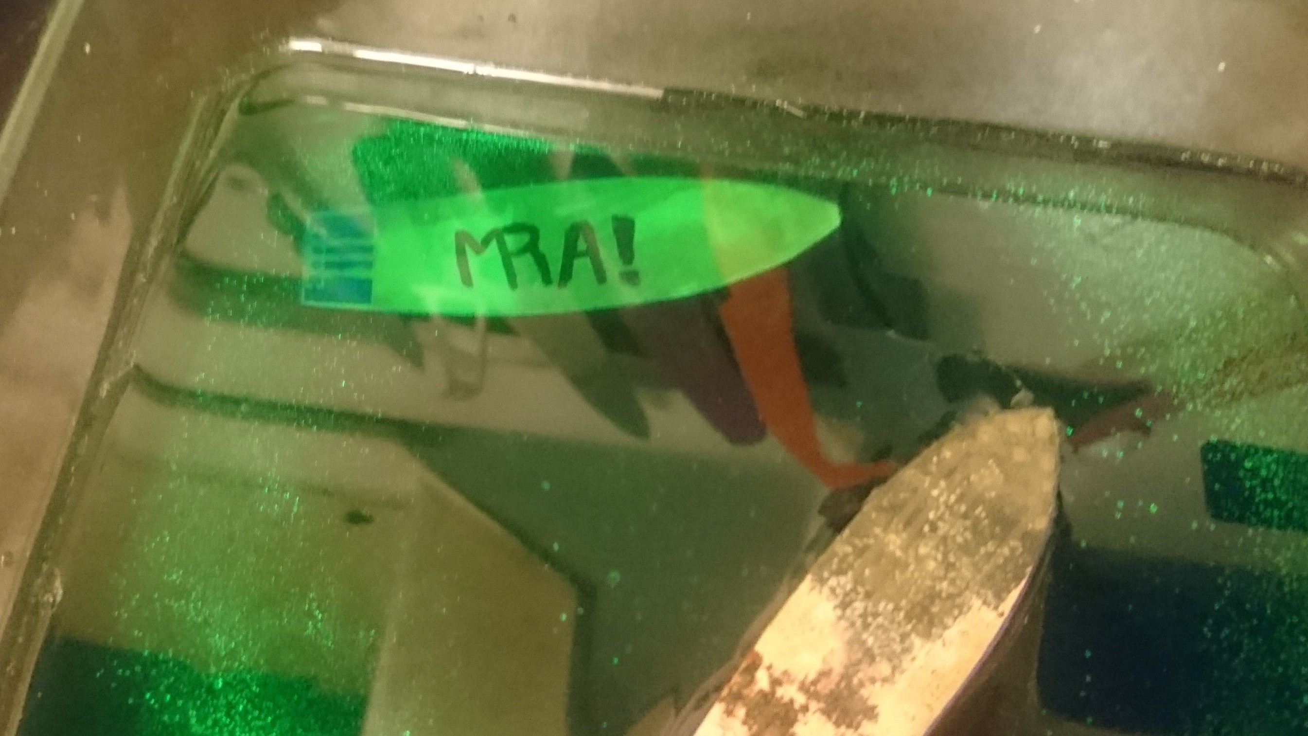
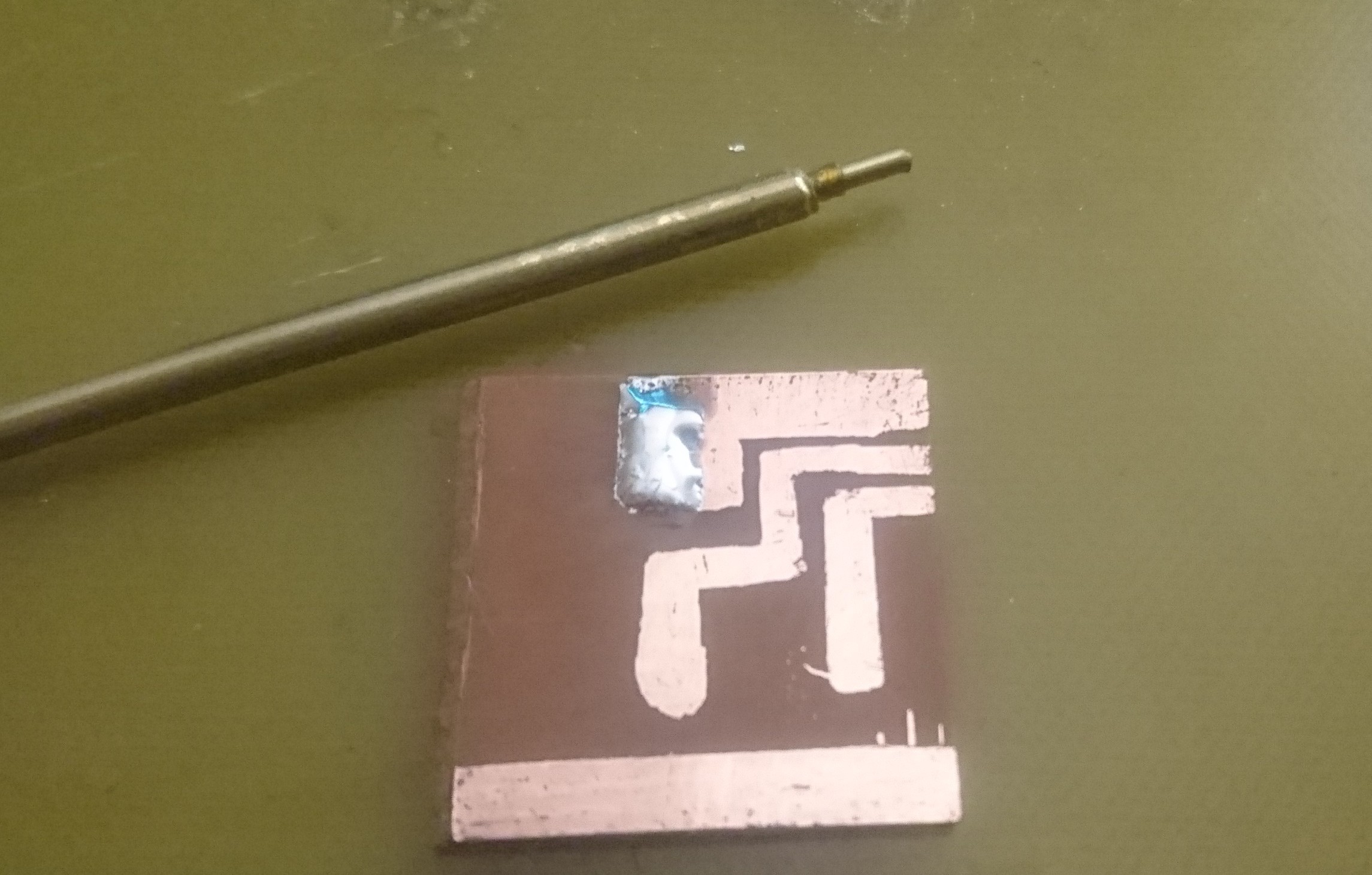
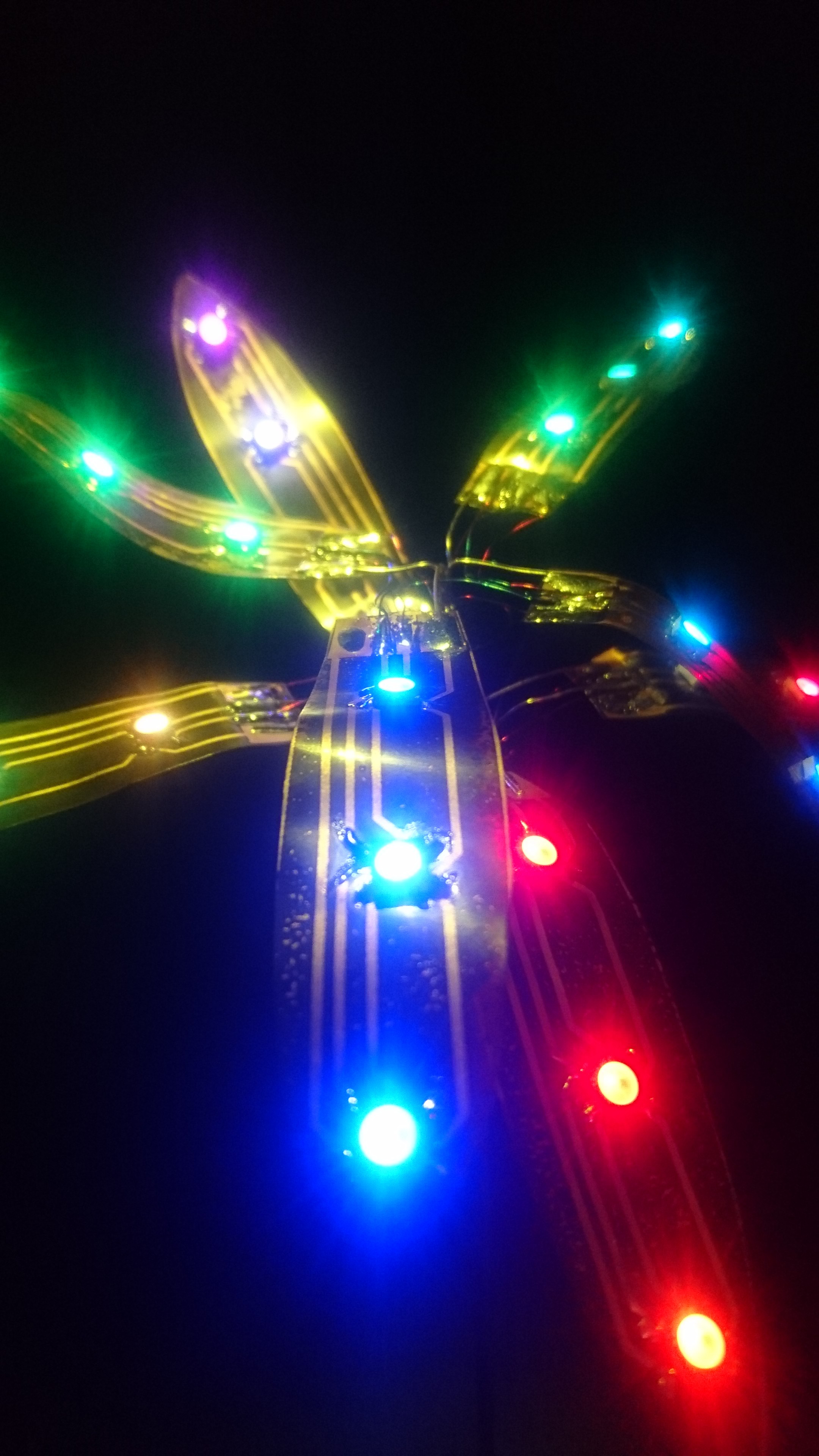
One of those other ideas was that I didn't want any wires showing but needed 3, power, ground and signal for the LEDs. After some complaining, shuffling around the house and drinking too much coffee it was decided I would etch one more board but only if I used SharpieCAD.
Here was the plan. Two brass tubes, one strand of magnet wire and a excessive use of fancy electrical tape*
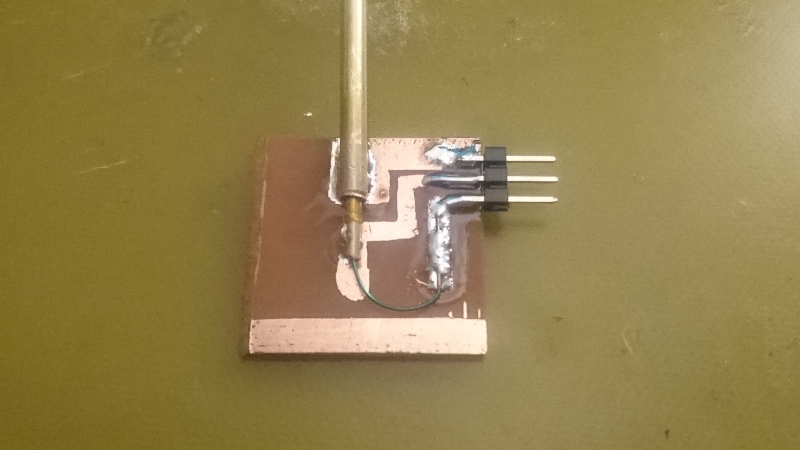
I was a little too pleased with myself at this point. Oh? That strip on the bottom you ask?
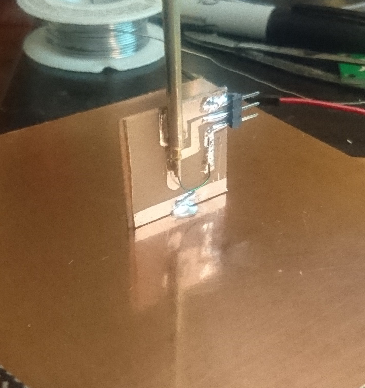
The top connection came out nice and organic looking.
With this the rest just sort of fell in place. I was pretty frazzled after 7 and a half days of working on this so I just went to town with a box cutter and a stack of copper clad while channeling @zakqwy . What a way to spend Sunday morning.
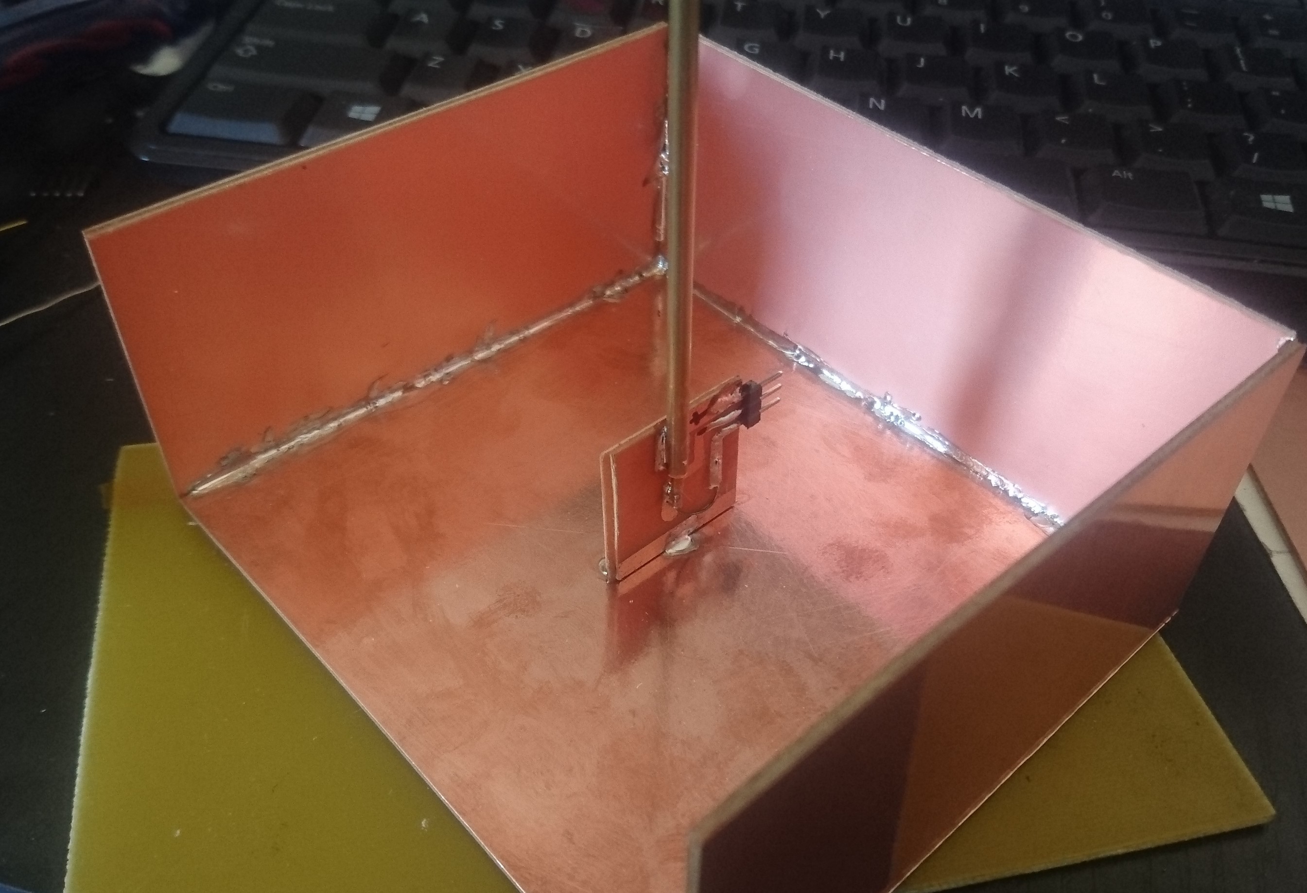
It's pretty easy to get clean cuts by heavily scoring both sides then snapping off on a table edge.
Welp, that's about it.

*) kapton