 Pero
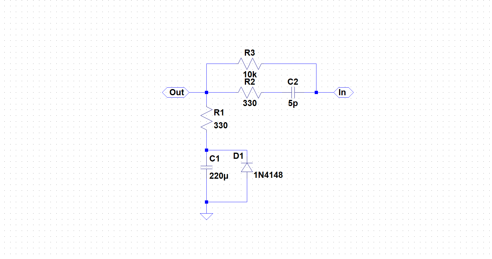
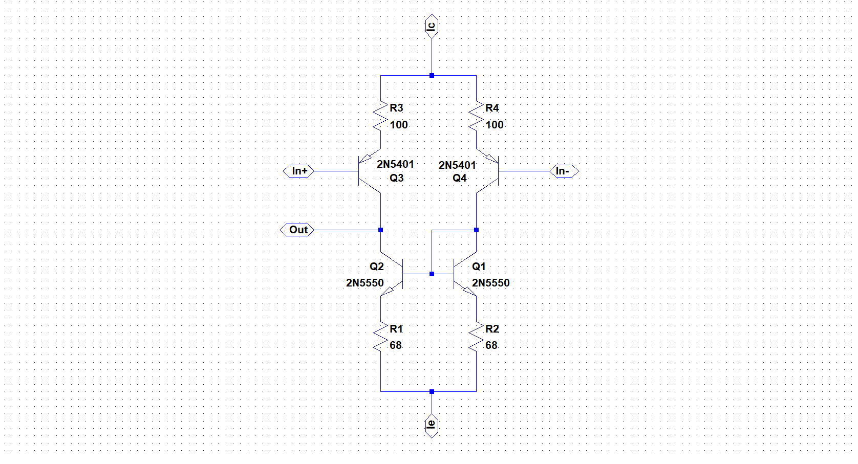
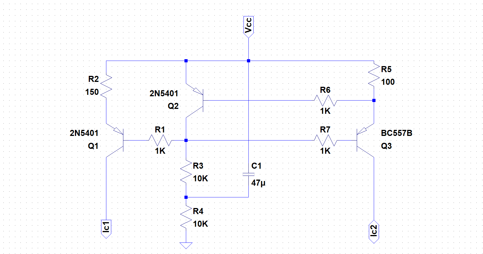
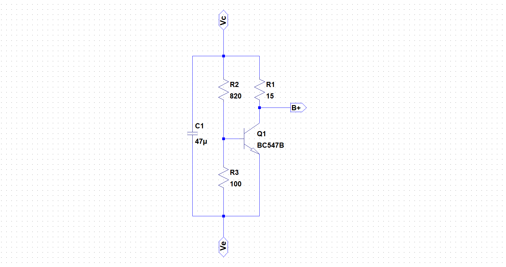
PeroI used LTSpice to examine inner workings of the circuit. I've made a block diagram of every main part of the circuit to simplify the schematics. There you can see an input diff pair stage, voltage gain stage, a current source that feeds them both, output power stage and a bias for the output power stage. I've even put a passive feedback network into the separate block.
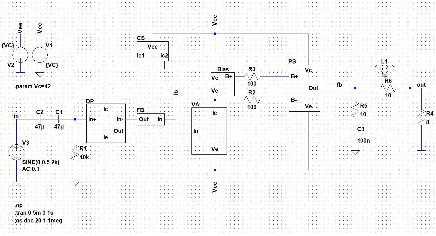
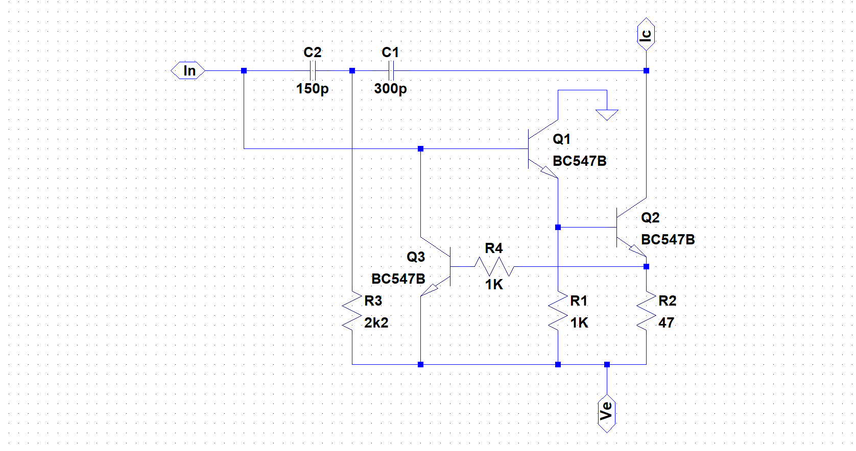
If you click on a block of every component, you'll find a corresponding schematic. I've used some ready made components available in the LT Spice library such as BC547 and BC557 bjts, instead of creating my own exotic components
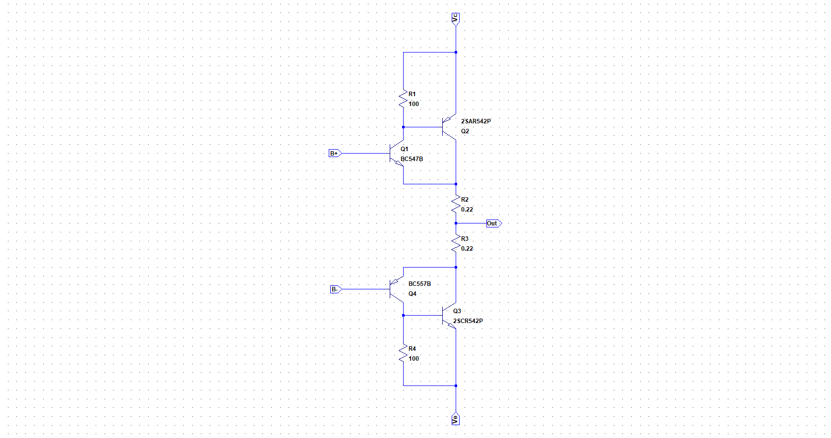
I've omitted the current protection circuitry from the power stage due to the simplicity.
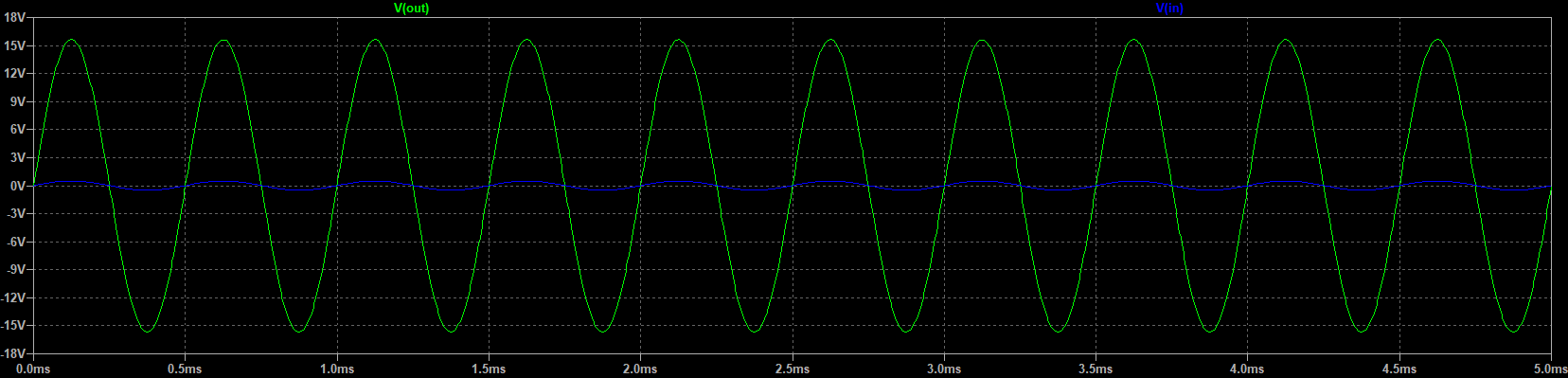
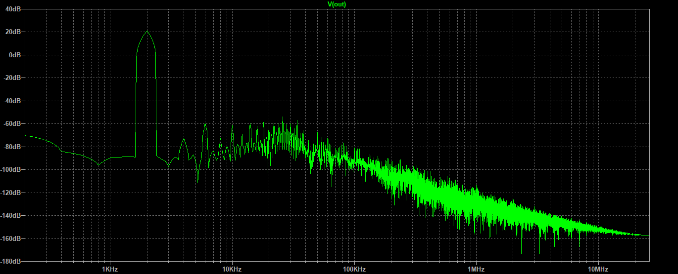
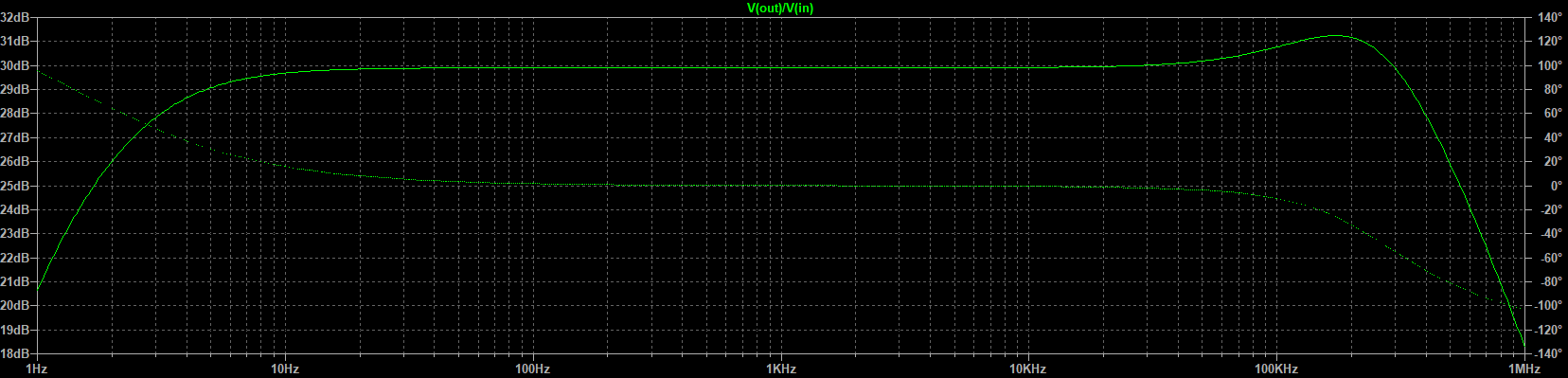
Simulation verified functionality of the amplifier. For a 2kHz sine input I got a clean sine output with a 30 dB gain. FFT diagram showed more than a 80dB attenuation of the 3rd harmonic. AC simulation showed a flat 30 dB gain over whole audio band.
One hugely important parameter that needs to be verified by the simulation is the bias voltage at the output stage. If the bias is too small the PS will fall into the crossover distortion as the output BJTs will cut off the current for too small voltages. If it is too high, the huge quiescent current will flow through the BJTs and eventually cause heating and/or destruction.
Discussions
Become a Hackaday.io Member
Create an account to leave a comment. Already have an account? Log In.