 David Pye
This clock is designed to multiplex the nixie tubes.
This means that only one tube is illuminated at any one time, and the code turns each tube on and off quickly enough that your eyes see them all as being on simultaneously.
A nixie tube has one anode, and a number of cathodes. Most numerical display tubes have 10 cathodes (digits 0-9) although some have as many as 12 (two decimal point cathodes - leading and trailing).
For direct drive designs the number of output lines from the microcontroller to drive the displays are 10 * number of tubes.
For multiplexed designs, the number of output lines required for switching is 10 + the number of tubes. So, for a 6 tube clock, a total of 16 output lines are required. Conveniently a pair of 74HC595 shift registers will provide 16 bits of output.
Advantage: Less circuitry + IO required, easier wiring
DIsadvantage: More software complexity and timing. Less bright for given current, so much higher current pulses are required to achieve the same brightness as a direct drive design, which may wear out the tubes more quickly (may - there are many different viewpoints on this!)
Most multiplex designs use the following basic design:
- Wire the same cathodes on each tube together. So, for example, each tube's 0 digit cathodes are connected together, each tube's 1 digit cathodes are connected together etc.
- To illuminate a specific tube, that tube's anode is driven HIGH (ie to the HV supply ~170V) to select it.
- The desired cathode is pulled to GND.
- A short blanking interval occurs where no anodes are pulled high, and the process then repeats for the remaining tubes.
- Cycle repeats
Microcontroller pins can't drive high voltage directly, so transistors are often used. Controlling the cathodes to pull them to GND Is easy, and can be done with a high-voltage capable NPN transistor, such as an MPSA42, like this:
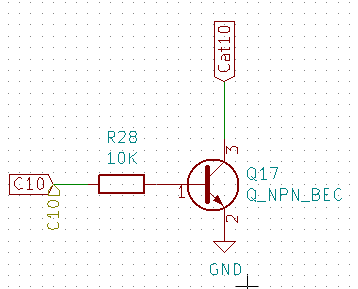
When address line C10 is pulled HIGH, the transistor conducts, and Cat10 here is connected to ground, illuminating that segment.
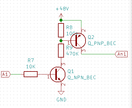
However, pulling an anode 'HIGH' to select a tube is harder, as this requires level switching. This design uses the following schematic: (+48V is actually +HV @ 170volts), and A1 is the address line. AN1 is the wired to the anode of Nixie 1. Q1 is an MPSA42, and Q2 is the PNP version (MPSA92).
So, when the address line A1 goes HIGH, the transistors switch, and 170V is applied to the tube's anode, thus selecting it.
So, the HV drive circuitry for this design consists of:
10 x the cathode drive circuitry
6 x the anode drive circuitry
(Actually, there is a spare cathode drive circuit, which you can use to drive some neon indicators for decimal points etc if you like!)
Discussions
Become a Hackaday.io Member
Create an account to leave a comment. Already have an account? Log In.
There's another configuration for the anode drive circuit that saves three base resistors, if you care. This "all your base are belong to us" configuration is described here: https://web.jfet.org/nixie-1/NixieTransistors.pdf I've seen it in use in my ancient Beckman clock (https://hackaday.io/project/160958-restoring-a-beckman-neon-display-clock). The drive inputs then become active low. Current handling of the MCU won't be a problem for you as you only need to sink enough current to drive the MPSA92.
Are you sure? yes | no