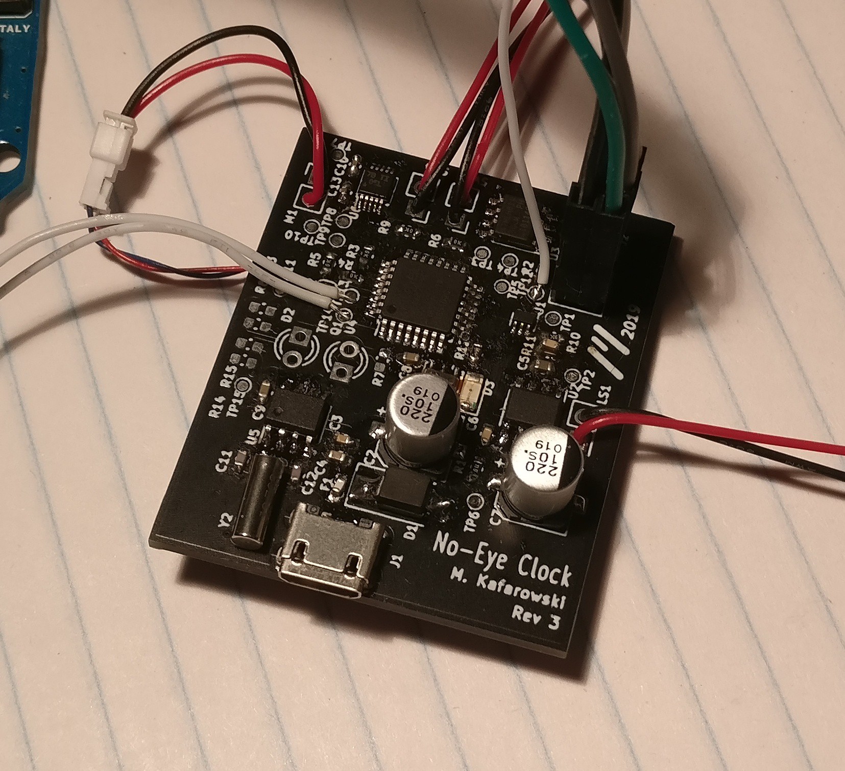
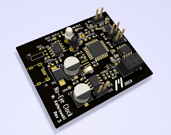
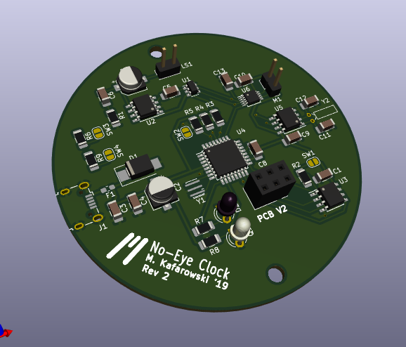
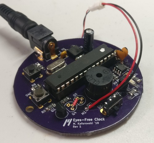
• V0.3 and the Audio Mystery Solved!

    Michael Kafarowski11/25/2019 at 03:18 0 comments

    I received the V0.3 PCB a few weeks after my last posting and was eager to assemble it and hear how much better the audio sounded now that I switched from I2C to SPI.


    I stayed up late soldering and programming a test program with the “PM” sound that was giving me issues before. After soft-bricking a few ATMega328PBs with incorrect clock source fuse settings, I got them right (it’s -Ulock:w:0x3F:m -Uefuse:w:0xFF:m -Uhfuse:w:0xD9:m -Ulfuse:w:0xCF:m for a 16MHz ceramic resonator), then I downloaded the firmware, plugged in the speaker, and…

    It sounded the same. The same distorted, shrill sound that I thought was related to I2C not being fast enough for 8KHz audio on V0.2.

    Over the past two days I’ve been troubleshooting the issue, going so far as to breadboard the whole audio circuit to prototype filtering techniques. I considered that the shrill noise may be coming from the the high frequency components generated by the discrete stepping from the DAC. I created a sine wave data pattern so that I could easily analyze it on the scope. After trying numerous hardware solutions, I found that configuring the audio path to go from DAC -> Passive RC (fc = 1000Hz) -> Buffer -> Voltage Divider -> LM386 -> Speaker produced semi decent results, outputting a pretty nice looking sine wave from my discretized input. The audio quality for the “PM” file was indeed better, but was pretty quiet and I could still hear a shrill noise.

    Turns out my mistake wasn’t in hardware at all, and that I was only right about I2C being too slow in theory. During troubleshooting I decided to try reexporting the audio files. This is when I discovered that the data I had previously exported wasn’t formatted as unsigned 16-bit words, but instead as unsigned 8-bit bytes. Because my code was expecting a 16-bit sample, in reality it was combining two separate 8 bit samples into one 16-bit word, which was then passed to the DAC. The meaningless combination of these samples caused the distortion. Because my data was already in a 16-bit form, I implemented a workaround that read the word twice, but passed the most significant byte, then the least significant byte separately to the DAC before moving on to the next word. The audio quality improved tremendously, and it sounded good even without all my new fancy filtering!

    I dug out my V0.2 board and implemented the fix in software. Although the sound was much clearer on this board as well, now that the audio was essentially playing at double the sample rate (two 8-bit samples needed to play for every original 16-bit sample), the I2C bus couldn’t keep up, and the audio took on a lower pitch than the original file, although the distortion had disappeared.

    This ordeal taught me the value in questioning my assumptions. I had already calculated that i2c would be too slow before I assembled V0.2 (but after I had designed it!). With this in mind, the fact that the audio was distorted seemed to make sense. But had I investigated a little bit more into the actual symptoms from basic level, I probably could have improved the audio quality in V0.2.
     
    Next steps:

    • Software
    • Test IR Triggering

  • Rev 3 PCB

    Michael Kafarowski09/04/2019 at 00:01 0 comments

    With revision 0.2 came some victories and some defeats. The audio system "worked", although the quality was quite bad. I chose an i2c flash and DAC chip, not realizing that the speed of that protocol was much too low for audio (<400kbps). I had to downsample my already low 8khz bandwidth audio track to <4khz, which resulted in a lot of distortion. To address this, I’ve chosen new parts, each now using SPI. As a matter of fact, the flash chip was the wrong choice anyway because it was a 3.3V part and my board runs on 5V. Oops. 

    I redesigned the whole board with smaller footprints, replacing the 1206 passives with 0603 for more flexibility and reduced size. 

    I also dropped the circular form factor for now, as it was an inefficient use of space. Once I finalize the circuit, I’ll decide on a final form factor and do a more thorough route.

    I've sent the board to fab, and it should be in some time next week.

    The project’s Github repo is now public! Check it out here: https://github.com/Aliasmk/NoEye-Haptic-Clock

  • Rev 2 PCB

    Michael Kafarowski06/05/2019 at 19:43 0 comments

    I've created a preliminary version of the PCB for the second revision. I still need to replace a few footprints and double check all the connections before sending it out. It's amazing how much extra you can fit when you don't have a massive DIP-28 taking up half the board.

    This is going to be a challenging board to build. I have never reflowed before, and I think that is going to be required for some of these tiny footprints. I've seen others place the PCB on a clothes iron to melt the solder paste, perhaps I'll give that a spin. I have a few weeks to figure it out.

  • Plans for Revision 0.2

    Michael Kafarowski06/03/2019 at 03:04 0 comments

    Revision 0.2 is under development. Hardware issues with the previous version are corrected (added load capacitors and a battery backup to the RTC). I’m also reducing the footprint of the parts as much as possible, moving towards more SMD parts and replacing the barrel connector for USB.

    As for major design additions in this revision, I am adding a haptic driver IC to enhance the experience in haptic mode. I’m also replacing the existing beeper with a speaker and will add an option to have the clock audibly read out the time in English using voice clips stored on a flash chip. The button to trigger the device will be replaced with either a non-contact light-based sensor or a capacitive sensor. The preliminary circuits are designed in schematic but I’d like to run a few electrical tests before laying out the board. After that I’ll layout the board and design a new case, then order the parts and PCB to put it all together. Here are some details about the new electrical features.
     

    Haptic IC

    Because the vibration pattern for reading the time digit-by-digit is complex (especially at first), it’s important that the vibrations being generated are of the highest quality. Crisp vibrations will make it easier to discern individual haptic pulses. I’m looking at the TI DRV2605LDGSR IC, which supports many types of haptic patterns and has drivers to overdrive and brake the motor for faster starts and stops. The chip is expensive though ($5.56 CAD) so it may be worth revisiting a more simple H-Bridge again to see if the performance is comparable.

    Audio Clock

    The audio clock function requires two components – the first being the audio system comprising of a DAC, an amplifier, and a speaker.

    Voice data will be stored in an external Flash chip in wav format. Given that mono, 12 bit wav files are be 60kB/s and we need a couple dozen seconds of sound (for each number, tens, teens, and words like “pm”, or “oclock”), a flash chip with a capacity between 1 and 4MB should be used. Flash chips, while slower and less flexible than EEPROMs, seem to be cheaper especially at high capacities.

    Trigger

    After using my v0.1 No-Eye Clock for a few months, I realized that I didn’t really like the button to activate the clock. It was awkward to push the button and hold the case in a way that was easy to feel the haptic vibration, and was sometimes hard to find the button in the middle of the night. I’m going to try out an IR/photo transistor sensor – when a hand is nearby, the reflected IR will activate the phototransistor and send a pulse to the GPIO. The IR LED needs only by pulsed every few sensors rather than stay on continuously, which reduces the power consumption of this sensor. 

    __

    Thanks for reading! Will continue to update!

  • Hackaday Prize Entry

    Michael Kafarowski04/12/2019 at 03:04 0 comments

    Hi! I've entered the No-Eye Haptic Clock into the Hackaday Prize for 2019. I'm hoping to learn and apply principles to take my project from a prototype (like it is now) to a production-ready product. I'll have a few months between when I finish school at the end of April and when I start my job in mid-July to devote time to this project. 

    I look forward to working and learning with everyone in this contest!

  • First Hardware Iteration Assembled!

    Michael Kafarowski02/23/2019 at 21:30 0 comments

    I recently ordered my revision 1 PCB, and got it back yesterday. With a few minor tweaks to the hardware and software, the system worked great on the first try!


    Last-Minute Tweaks to the Rev 1 board

    • I forgot to add load capacitors to the 32.768 MHz RTC crystal. The particular crystal I had purchased specified a 12.5pF capacitor. The closest I had to this were 10pF ceramic caps, which I surgically inserted between each lead and a nearby ground pin. The mismatched caps will probably change the crystal's frequency slightly and cause the clock to run a little slow or fast. I'll keep an eye on this.
    • Removed two mosfets that were to have formed a half H-bridge for the haptic motor. In testing between when I ordered and received the PCB I didn't feel any difference between passive and electrical braking of the motor.
    • Some pin changes were needed in software from the breadboard version.
    • My breadboard version used a different I2C RTC - the DS3231 instead of the 7940N on the PCB. A 7940N library dropped right in and worked like a charm.

    Next Steps

    There are definitely a few improvements to make on the next revision. Now that I am confident with the circuit I'm going to try to reduce it's footprint, that means replacing the massive DIP-28 and beeper packages with smaller, probably surface mount parts. I'm also going to implement the battery backup on the RTC. I also have plans for other features, such as a clap detector circuit or a low-energy conversion so that the circuit can be used with batteries (perhaps as a watch).