 5Volt-Junkie
Project Write-Up
Tiny note: maybe my English sucks a bit, but I hope you can understand the most of the text below :-)
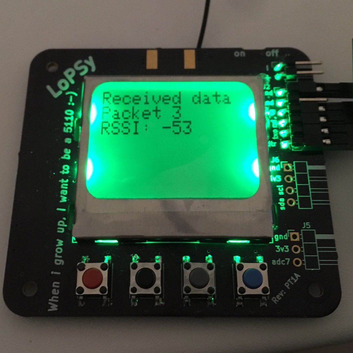
A couple of months ago, I wanted to experiment with LoRa modules. I started with a breadboard, two AI-Thinker Ra-02 LoRa modules, Nokia displays and ATmega328 boards. After a couple of experiments, I designed a tiny board, my first LoRa pager.
I played around with the new board for a while, made some range tests and got some ideas for improvements.
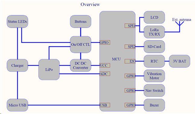
In the second version of the board, I wanted to keep the board Arduino compatible, but needed a better microcontroller, so I used a SAMD21 Cortex M0 (same on Arduino Zero MKR) microcontroller instead of ATmega328p. I was a bit unhappy with the Nokia display and replaced it with a bigger one. The availability of the AI-Thinker Ra-02 module isn't as good as the RFM95 and I also wanted to get rid of the U.FL connector. So the three main components were replaced and I needed some more features like LiPo Charger, real time clock, sd-card, a proper on/off circuit, navigation switch instead of common push buttons and a buck/boost-voltage converter. I also added some nice-to have things, eg. vibration motor and buzzer.
While designing the schematic, I decided to pick components, which I can get from the common big distributers for electronic components. I decided to choose all the components from Digi-Key, so I can save some shipping costs.
(I don't want to write the detailed hardware description here. For hardware details see the "LoRaNicator Hardware Description" below.)
After 10 sheets of schematics drawing, I started to design the two layer board and configured the design rules first. I used following (significant) design specs which are compatible with the most pcb manufacturers (OSHPark, JLCPCB etc.)
Min. Trace Width / Clearance 6.3mil (0.16mm)
Min. Via Drill / Outer Diameter 10mil (0.254mm) / 20mil (0.508mm)
For the power rail I've chosen a thicker traces: ~23mil (0.6mm). There are two interfaces, where the impedance controlled design has been required. The antenna trace and the USB differential pair.
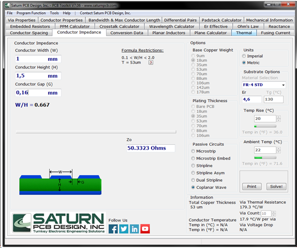
For those kind of trace design I like to use the PCB Toolkit. Since the board is a two layer design, with 1.6mm thickness, I neglected the USB differential pair to avoid crazy thick traces. The USB traces are pretty short, so it shouldn't make any trouble.
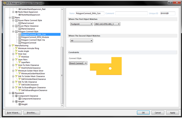
I only focused on the width of the antenna trace. The transmission-line I decided to go with, is coplanar waveguide with ground plane (GCPW). I entered the substrate thickness of the pcb (1.5mm / 59mil) and the overall clearance 0.16mm (6.3mil) and calculated 1mm (~40mil) for the trace width to get a 50Ohm impedance.
I also modified the signal pad of the SMA connector (same width as the trace) to match the 50R impedance. I added a rounded corners to the pad and added a copper cut-out at the edge, next to the signal pin. Furthermore I added a via fence around the GCPW.
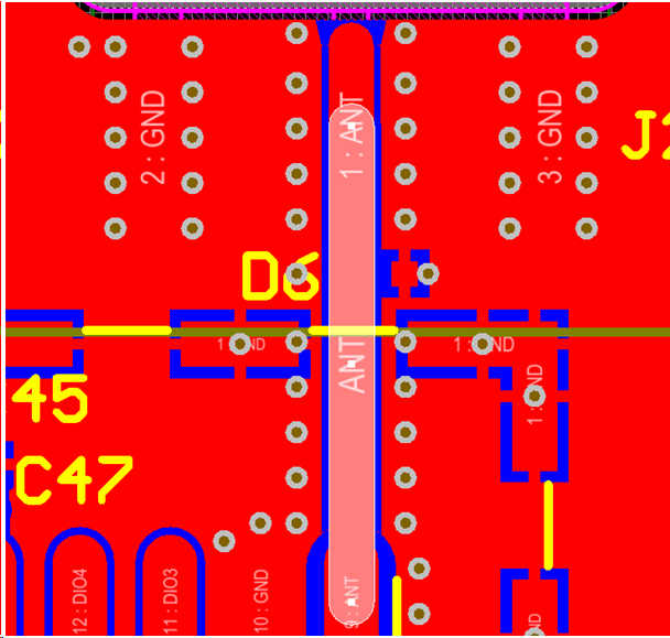
A good ground connection is also a factor to improve the HF design. So I created a special design rules in CurcuitStudio, to make a solid connection to GND pins of SMA connector and the RFM95 module. The ground connection for all the other components has the relief connection format
Also placed a lot of vias, for direct connection to the ground plane on the other side of pcb. Maybe it will improve the HF performance or maybe not, but I placed a shield can over the RFM95 module.
After designing the schematics and pcb, I ordered the board and a stencil for reflow soldering. The boards came with a gold finish and black solder mask and looked pretty nice :)
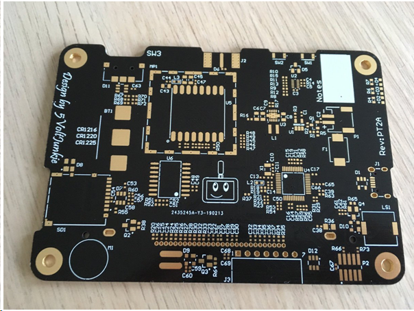
There are about 180 components on the board and many resistors and capacitors in 0402 package. So I didn't want to solder it by a hand and decided to use a reflow oven. I placed all the SMD parts expect the LoRa module and parts with a relatively bigger amount of plastic (JST connector, nav switch, SWD connector etc.) I melted a couple of plastic parts during the reflow soldering in the past. I also realized the influence of the soldering mask to the reflow process. I didn't have any soldering issues in the past, when I ordered PCBs with green solder mask. Now, the solder mask is black and the reflow oven uses an infrared heater and as we know, dark colors heat up more than light colors... ;) Long story short, the solder paste has been overheated a bit. Take a look on the picture below and you will notice a gold / brown surfaces on the soldering pads.
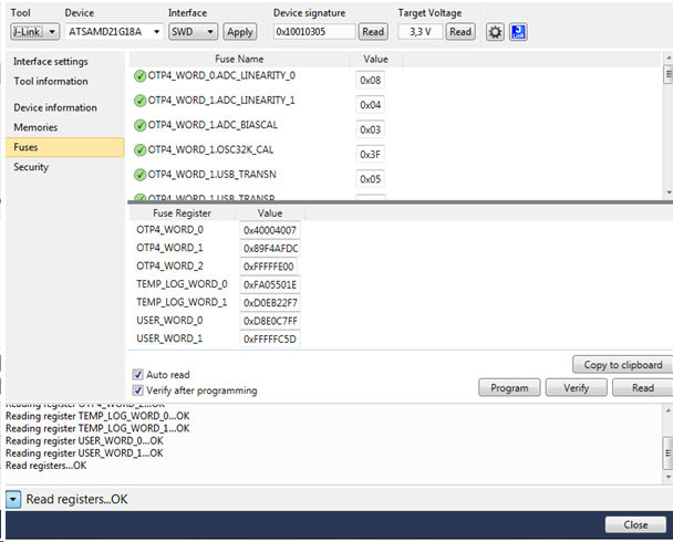
To burn the Arduino bootloader to the SAMD21 microcontroller I needed an appropriate programmer. The Atmel ICE is a bit too expensive for me, so I ordered a Segger J-Link EDU Mini https://www.segger.com/products/debug-probes/j-link/models/j-link-edu-mini/
After the driver installation I was able to chose the device in Atmel Studio and burn the bootloader
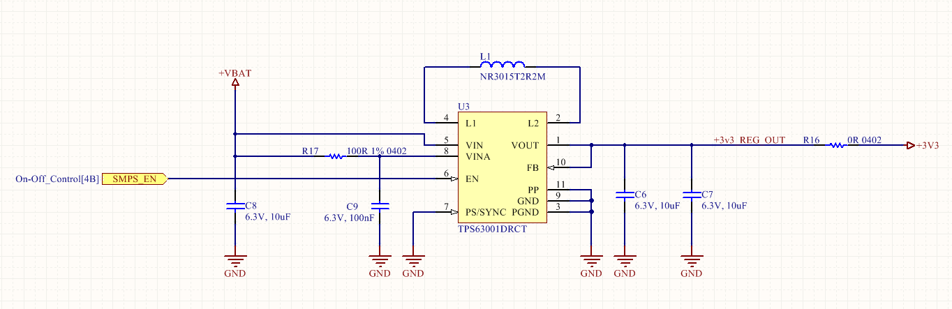
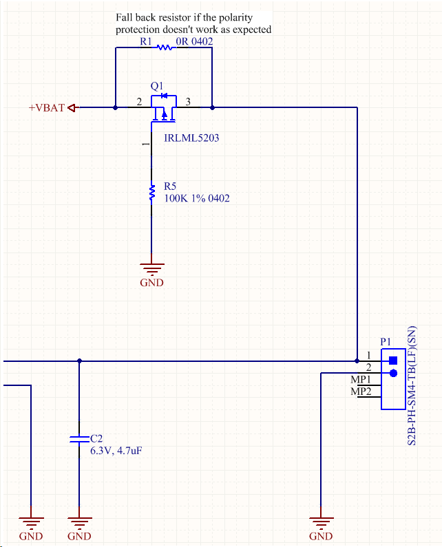
Before I burned the bootloader, I realized a little imperfection in my design. After pushing the power button on the LoRaNicator, the On/Off controller enables the 3.3V source and is waiting for a feedback from the microcontroller (HIGH signal) for a short time to keep the 3.3V enabled. If there is no feedback from the µC, it disables the 3.3V and bye-bye! I disconnected the 3.3V output of voltage converter from the rest of the circuit by removing the R16 0R series resistor (see schematic below).
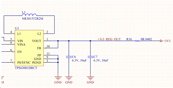
Now it was more safe to power the board with an external 3.3V power source and avoid any damages to the onboard voltage converter.
So we speak about troubles and issues. Let's proceed with this topic ;)
After I burned the Arduino MKR Zero bootloader to the µC, I wanted to test the SRC0 On/Off-controller. I flashed a simple sketch where I set the feedback pin for On/Off controller to high. Nothing more. It didn't work. The problem was, that the SRC0 enables the 3.3V only for 2 seconds, but the SAMD21 needed a longer time window (~2.5seconds) for powerup and set the feedback gpio (PShold) to HIGH level. I scrolled the SRC0's datasheet to the bottom and noticed that they have another version of this IC, which enables the 3.3V for ca. 10 seconds. I ordered it, desoldered the old one with hot air gun, soldered the new one with the hot air gun again and it was fixed. During the waiting for the new part, I used a workaround by attaching a 10k pull-up resistor to the PShold gpio, so this pin stays HIGH after the power up. There was just a little voltage drop in the moment when the controller switches the default high impedance state of the gpio to output and high level. However, this very short voltage drop on PShold didn't affect anything (probably due the debounce time of SRC0's). So before the new SRC0 IC arrived, I was able to test another function and spot some other issues. Unfortunately, I was a bit nervous during the investigation and debuging of this power up issue and I forget to make some screenshots on my oscilloscope :(
Charger, Display, RTC, LoRa module, buttons, SD-card, voltage converter. All worked well. But not the RTC. I flashed the microcontroller with different sketches and used different libraries and I tried out the I2C scanner. Nothing worked. I measured the signals with the oscilloscope and noticed a voltage around 0.3-0.7V on SDA & SCL and a small jitter on SCL. "0.3V - 0.7V? Must be something with diodes!"- was my thought. I noticed the ESD protection diode array for external I2C devices was misaligned.
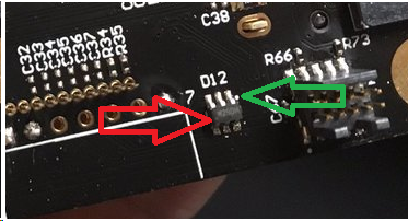
So I desoldered it, rotated for 180° and soldered it again. The RTC still didn't work. Maybe I destroyed the RTC IC during the reflow process or during some earlier tests?
I desoldered the 39R series resistors R53 and R54 and connected the original Arduino MKR Zero to LoRaNicator's RTC, because I thought the RTC were broken.
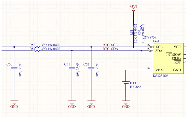
It worked well. I opened my schematics and found TWO mistakes. The first one was my opinion, that the RTC circuit is sooo simple, I wouldn't make any mistakes. This attitude was the biggest mistake! But I fixed it by scrutinizing my opinion and by reading the schematics. Aaaand here we go! I interchanged the I2C wires SDA & SCL. F@cK MY LIFE!
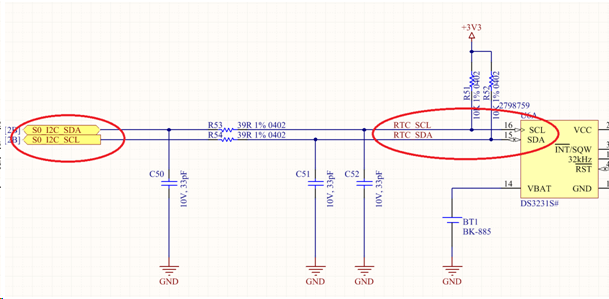
I used short pieces of coated copper wire to fix this problem and then the RTC worked properly.
LoRaNicator Hardware Description
Power
The pager can be powered by a single LiPo cell. Theoretically, it can be powered by any power source within a voltage range of 1.8V to 5.5V. Practically the board was designed for a single cell LiPo, so the onboard charger can charge it via USB, but could cause damage to the board and / or to the battery if you use something else instead of the LiPo cell. The battery’s output voltage will be converted by a TPS63001 PMIC to +3.3V DC on-board voltage, which is the operating voltage for all components on the board. The regulator’s output current can go as high as 1200mA (absolute maximum) and operates at up to 96% efficiency.
Charger
The charger IC is a MCP73831T and can charge the 1-cell LiPo via a USB cable. The charging current is adjustable with a resistor (R3). The standard setting for the charging current is 100mA. I recommend not to charge with a current over 400mA, since there is also a 500mA resettable fuse (F1) in USB +5VDC VBUS on board. Further, the charger have a status LEDs (D2, D3). The red one for charging state „Charging“ and green for „Charge Complete“. The battery voltage is connected to an ADC pin via a voltage divider the same way as on Arduino Zero MKR (330k and 1M2). At ~4.2V LiPo voltage, the ADC measures ~3.3V on the voltage divider.
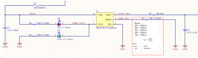
There is also a simple reverse polarity protection for the LiPo cell. Honestly, I didn't tested it yet, what happens if the LiPo is connected the wrong way. But this circuit did work in another applications. I will test it when the second board is finished ;)
On/Off Controller
The LoRaNicator contains a SRC0 On/Off-Controller that provides the possibility to turn the device ON or OFF by long press of the push-button (PB).
Power Up
To turn the device on you have to perform a long push of the Power Button. After a debounce time (ca. 30ms) the enable pin (EN, output) of SRC0 drives from LOW to HIGH. Since this pin is connected to the enable pin of the voltage regulator, it enables the +3.3V power rail. When the +3.3V is up and running, after a short delay (240ms-480ms, but typ. 360ms) the SRC0’s reset output pin, connected to the reset pin of the SAMD21 microcontroller goes HIGH. That action provides a clean reset of the microcontroller. While you keep the PB pressed, the microcontroller’s pin PB03 (Arduino style A2) has to be set to output and to the state HIGH. This pin drives the PShold pin of the SRC0, like a „I’m alive!“ status. At this point the button can be released. The voltage converter will be kept enabled as long as the PShold pin is HIGH.
Power Off
The device can be disabled in two ways, from the microcontroller by driving the PShold signal LOW or by long press of the push buttons PB and SR. By long pressing the PWR button , the SRC0 performs an interrupt signal on INT (low active) pin. Then the interrupt routine can be triggered. In this routine you can define something like a „Confirm Shut Down?“ dialog or just set PShold to low. That would disable the +3.3V and the whole device
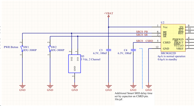
SmartReset and PBout
It's also possible to perform a hard shutdown by pressing both buttons simultaneously. The time how long both buttons have to pressed is defined by C4. Just calculate the time period with 10s per µF. I decided to set it to 100nF = 1 second.
The PBout pin of SRC0 is connected to the microcontroller’s pin PA04 (Arduino style A3).
RFM95W
The RFM95W module is connected to the S1 SPI together with the LCD. The CS pin for the RFM95W module is connected to micro controller’s pin PB22 (Arduino style: 14). The DIO0 pin (IRQ) of the RFM95W module is connected to microcontroller’s pin PA20 (Arduino style: 6). The RST pin is connected to PB23 (Arduino style: 13). The rest of the RFM95W’s I/Os are also connected to the microcontroller.
| RFM95W Pin Name | SAMD21 (Arduino) Pin Name |
| RST | 13 |
| NSS | 14 |
| MOSI | 8 |
| SCK | 9 |
| MISO | 10 |
| DIO0 | 6 |
| DIO1 | 2 |
| DIO2 | 7 |
| DIO3 | A0 |
| DIO4 | 5 |
| DIO5 | 3 |
LCD
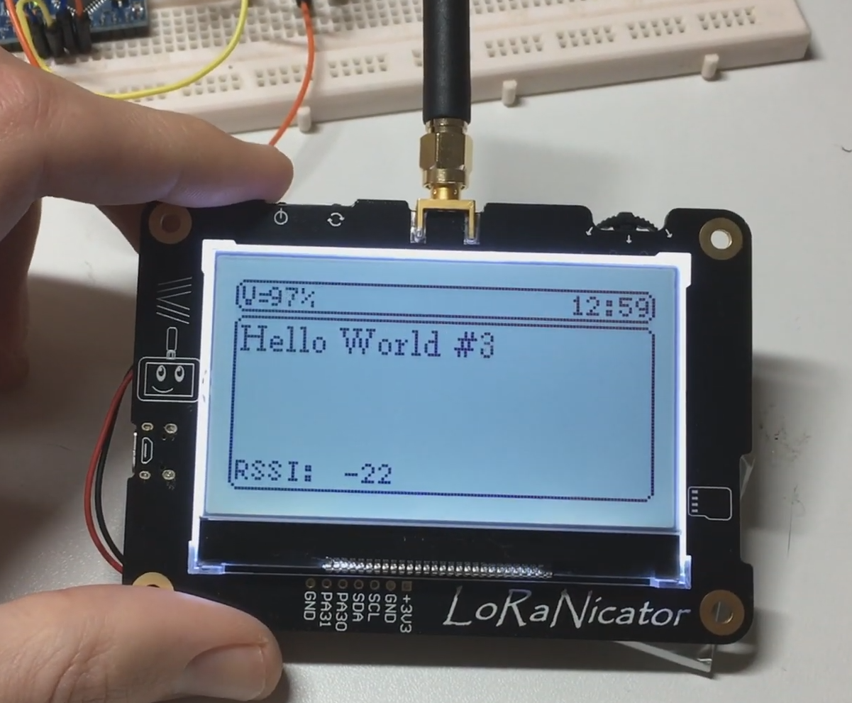
The LCD is a 128x64 pixel monochrom display (NHD-C12864LZ-FSW-FBW-3V3) with white backlight (I also have the negative version of it but not tested yet). It’s connected to the micro controller via SPI (MOSI, SCK) and some additional control pins (chip select, register select and display select). To control the display I’ve found a very nice Arduino library written by Oli Kraus. https://github.com/olikraus/U8glib_Arduino
It supports dozens of Displays with a very wide function range and is well documented.
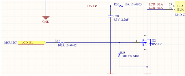
The display backlight is connected to a N-channel MOSFET and can be controlled via a GPIO.
The LCD is connected to the same SPI lane as the RFM95 module.
| LCD Pin Name | SAMD21 (Arduino) Pin Name |
| SCK | 9 |
| MOSI | 8 |
| CS | A4 |
| RES | A5 |
| A0 | A6 |
| Backlight (through a MOS-FET) | Onboard LED |
RTC
Of course you can receive the time from your LoRa transmitter, but I wanted to add the possibility for having a „local clock“. I selected a pretty expensive RTC (DS3231S) with external battery to avoid a time reset in case the LiPo battery has to be disconnected for some reasons.
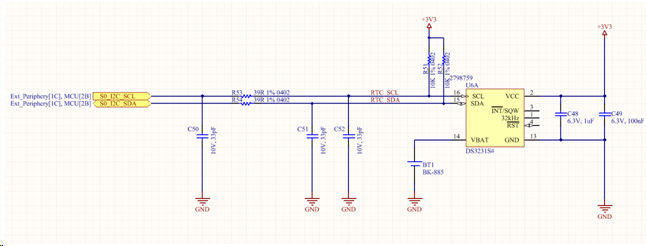
As I mentioned above, there was a wrong wiring of SDA & SCL pins. I fixed it in the HW rev. PT2B.
SD-Card
The micro SD-card is connected to a dedicated SPI bus and also have a card detection pin. It's connected to the microcontroller the same way it's connected on the Arduino MKR Zero.
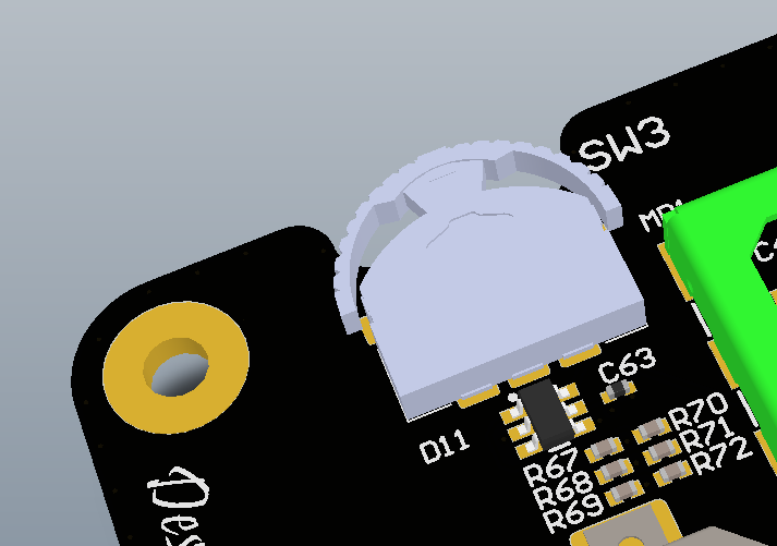
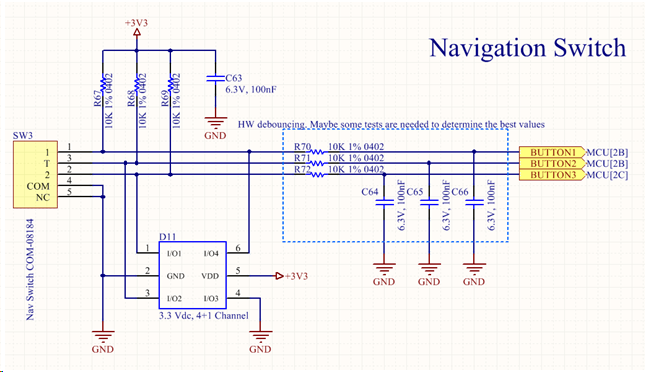
Navigation Switch
The navigation switch contains three internal push buttons for three directions, left, right and down. The down direction is designated for confirmation (e.g. OK or Enter). All three buttons of the navigation switch are connected to three GPIOs of the microcontroller. Each button have a pull-up resistor to 3.3V and pulls the signal level low if the button has been pressed.
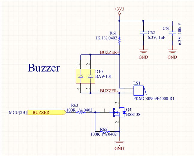
Buzzer
The buzzer is a pretty quiet one and I noticed it a bit too late. It is connected to a N-channel MOSFET and can be controlled with a PWM signal by GPIO. If the SMD buzzer is to quiet, it could be desoldered or not populated and another one can be connected with two wires or something like this.
ESD Protection
I would like to design a small case for LoRaNicator, but some interfaces will be still accessible by a user and to avoid an ESD damage, I placed ESD protection diodes to these interfaces. Antenna, SD-Card, USB, Buttons and the pin header for external periphery.
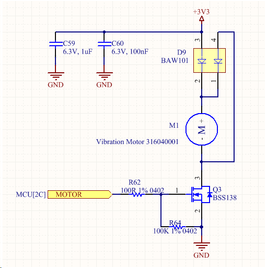
Vibration Motor
There is also a vibration motor connected through a MOS-FET to a microcontroller's gpio.
SWD
Through the SWD connector the Arduino bootloader can be flashed. The SWCLK and SWDIO are also connected to the pin header for external periphery. I hope to be able to connect a tiny keypad to the LoRaNicator.
Connector For External Periphery
Besides the SWD pins, the header for external periphery also have the I2C. Maybe it would be possible to connect some daughter boards, like GPS, keypad or some humidity sensors. We will see :)
I made some short clips during the project development and a short demonstration :)
Want to build your own LoRaNicator?
In the Details section of this HaD project I shared the Altium CircuitStudio Project Package for LoRaNicator. You can also find the 3D files, the Gerber files and so on. I didn't figure out yes, how to import CircuitStudio Project in CircuitMaker, so more pepople can view the schematics and pcb design files. I'll try to import it in Altium Designer and then import it in CircuitMaker. On the photos and in my videos you will see the hardware revision PT2A. This is the version where the I2C signals were crossed. In the hardware revision PT2B I fixed this I2C issue.
I also creatad a Bill of Materials on Octopart. I sourced all my parts from Digi-Key, but there you can also take a look on different distributors and their stock. To make the BOM more clear, I added the component designators in the row "Schematic Reference".
However, the letters PT (PT2A, PT2B) stands for prototype, so build it on your own risk!!!