As discussed in the previous log, I wanted to build this project with components at hand. This, combined with issues in amplification meant I would have to use a N-channel MOSFET as a high-side switch. I knew that this wasn't the common application for N-channel MOSFETS, but I never understood why. Here is what I learned:
First, let's look at the problem. A MOSFET is controlled by the electric charge on its gate, in respect to the source. Basically, for a N-channel MOSFET, you need your gate to be at a higher potential than the source (a positive Vgs) for the transistor to turn on. In my case, the Vgs required to turn on the transistor is about 4.5V, that is; the gate needs to be 4.5V about the source.
This is the reason that N-channel MOSFETS are generally used as a low-side switch. Any (positive) voltage at the gate will be at higher potential than the source, because the source is connected to ground. This is not the case when in the high-side configuration. Let's take a look:
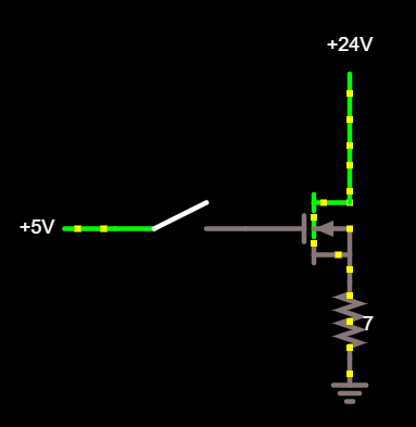
If you are like me, and have a limited intuition about these things, this configuration looks like it would work fine, When the switch is closed, the gate will be at 5V, and the source is at 0V, so what's the problem?
When the the switch is closed, the transistor does turn on, however, the voltage across the resistor cannot rise above Vgate - Vgs_threshhold (5V - 4.5V). This results in the load having 0.5V across it, and we get 0.5V / 7ohm = 71mA through our load. Far from enough to drive a soldering iron.
What if we use the supply rail to drive the MOSFET? Let's look at the following configuration:
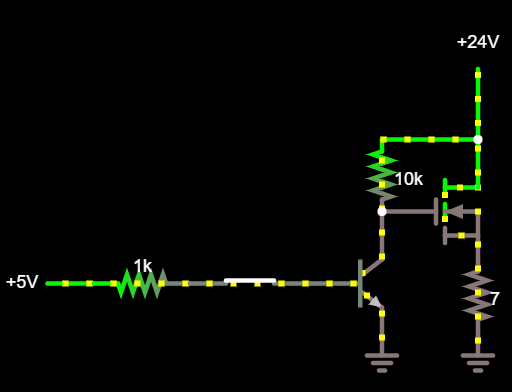
Here, we use a NPN BJT to drive the gate of the MOSFET. When the BJT is ON, the gate is pulled low, and the MOSFET is off. When the BJT is OFF, the gate is pulled to the supply rail through the 10k resistor.
Great! Now we have 24V at the gate, surely that solves the problem! But no, this makes our problem worse.
When the gate is pulled to 24V, the MOSFET turns on and passes current through to the load. But once again, the voltage across the load can't rise above Vgate - Vgs_threshhold (24V - 4.5V = 19.5V). This results in 2.8A through the load. Great, but wait! What about those 4.5V that are missing across the load? They don't magically disappear. Instead, they are dropped over the MOSFET. 4.5V * 2.8A is over 12W. That's way too much. Not only would the MOSFET heat up far to much, but we also lose 15% of our theoretical max power of 82W.
Here's what I did:
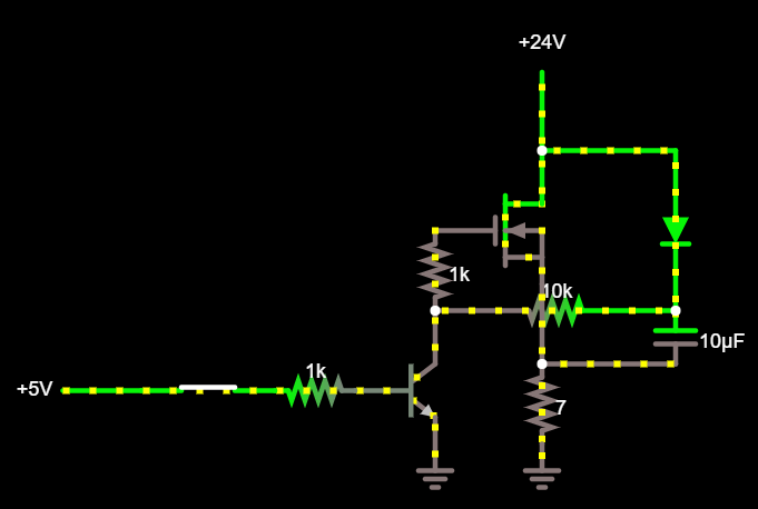
We can use the capacitor and diode on the left side of the diagram to "capture" the potential difference over the transistor when the transistor is off. The capacitor charges through the diode, until there is 24V across it (minus the forward voltage of the diode). The NPN BJT is initially on, which means the gate of the MOSFET is pulled low and will not conduct. When the BJT is turned of, the voltage across the capacitor is transferred to the gate of the MOSFET, turning it on. This is where the magic happens.
As the potential across the load rises, the potential at the negative side of the capacitor rises. The cap can not discharge (bar reverse leakage current of the diode and leakage current through the gate of the MOSFET), so it will maintain 24V volts across it. This means that if there is 24V across the load, we have 24V+24V (ideally) at the MOSFET gate! Perfect, now we have produced a Vgs of 24V, plenty to keep the MOSFET fully on. (Careful though, Vgs has an upper limit, and overloading it can damage your MOSFET).
I copied this solution straight from this video by Julian Ilett and this one by 0033mer.
In conclusion: There are pros and cons with using this configuration for high-side switching.
Pros:
- N-channel MOSFET's are more widely used, and one might be more likely to have one at hand.
- Lower on resistance, leading to higher efficiency and less heat.
- Easy to drive
Cons:
- Large number of components (all though they are all what I would consider jellybean parts)
- Not suitable for higher frequencies. (I haven't calculated or simulated this but it does need quite a large capacitance to work, and that is rarely great at higher frequencies).
- Potentially harmful to the MOSFET if the Vgs is too high.
Discussions
Become a Hackaday.io Member
Create an account to leave a comment. Already have an account? Log In.
Hi all.
Thanks for writing this. I have been reading more than 20 explanations on this bootstrap concept with an n-channel MOSFET on the high side and I kept mentally rejecting the explanation like a splinter in my mind.
I finally understood it by deleting everything I read and experimental setups on YouTube out of my mind. It puzzles me why they didn't measure the gate voltage relative to source pin to test their theory? That is the variable in question. They measured gate to ground potential.
So, in steps using the last diagram shown above - a simplification ignoring transient effects and non-linear nature of diodes:
*** TRANSISTOR ON = MOSFET OFF ***
1) The transistor is on.
2) So all the current (conventional) flows through the green path, in this case from +24V to ground through the transistor.
3) This charges the external capacitor to +24V. The gate capacitor will be floating at the last voltage before the circuit was switched off, but in a PWM scenario, it would have been discharged to 0V relative to ground and source in the previous half-cycle.
4) Since the external capacitor has +24V on the positive plate, the other plate is at 0 Volts relative to circuit ground. This is the important bit. The negative capacitor plate is referenced to ground *potential* via the load, but no current flows across the capacitor (a parasitic amount through the load) as it is "DC". Even though it will be used in a PWM scenario, this is a modulation of DC *potential* and not a reversal of polarities like AC, although it has a DC modulation frequency when the circuit is running freely.
*** TRANSISTOR TURNS OFF = MOSFET STARTS TO TURN ON ***
5) The 5V PWM signal from a 555 timer or Arduino or computer, etc brings the base of the transistor low and thus switches it off. There are a few ways to use transistors and each can be either PNP or NPN so this is assuming you selected a transistor and wired it up to act as a low side switch that switches off current flow when the base is pulled low by a timer. As per the diagram.
6) There is now no path to ground through the transistor.
7) This forces the gate capacitance of the MOSFET to be charged to 24V.
8) *** CRITICALLY *** the point in the circuit where the external capacitor positive plate and the gate capacitor positive (negative is relatively the PN g-s junction) are both connected ARE AT A POINT OF EQUAL POTENTIAL. i.e. they are BOTH AT Vcc or 24V in this case.
9) This is because as the gate capacitance begins to charge, there is an infinitesimal flow of charge to the source pin of the MOSFET. Thus it has effectively infinite resistance compared to the 10k and 1 resistors. So the gate pin sees Vcc (24V) as does the external capacitor positive plate. Relative to the source pin.
10) At no point does Vcc get doubled or increased by the external capacitor at all relative to the source pin. Explanations say "compare it to a battery in series with Vcc causing a doubling in voltage" - or words to that effect. We have to remember what potential is and a potential difference before we talk about things like this. If you connect the positive poles of two equivalent batteries in series, the point in between the two batteries is half the total potential difference. I remember asking my teacher in school this question and was just coerced into accepting the wrong theory and shown a working circuit in practise. Subtle and easy to miss this when in a hurry to complete a project or place an order for parts.
11) The gate capacitance positive plate starts to get charged by Vcc mainly.
12) The gate capacitor reaches and exceeds the designed potential of Vgs given in the MOSFET datasheet (1V for my particular MOSFET) and if the MOSFET is kept on long enough (micro to milleseconds depending on the MOSFET) it can reach almost the full value of Vcc (minus Vdiode).
13) At the point in time that the gate potential reaches Vgs, the MOSFET conducts current. Typical MOSFETs have graphs to show current flow at different gate potential differences: Vgs.
14) The reason current flows is because the threshold of Vgs has been reached. So the gate would be at a higher potential than the source for this reason. NOT because of an increase in Vcc. The existence of the load resistance would have it "see" Vcc at the top connection of the load so the potential across Drain to Source would be almost zero before conduction. You can think of the negative plate of the capacitor as a "virtual ground" that is always connected to the source pin.
***MOSFET FULLY ON***
15) Now that current is flowing through the MOSFET and the load, there is a tiny voltage drop due to Rds(on) at the source pin, called Vds which is negligible in this consideration. There is a voltage drop across the diode at all times it conducts, call it Vdiode that is less than Vcc.
16) The source pin is effectively at the mid point of two potential differences (akin to being between two batteries in series). The first with the capacitor in parallel with Drain and Source, the second between the conducted Vcc and ground via the load. Each off these potential differences is 24V with the mid point being 24V relative to ground.
17) The diode and capacitor cause this relationship because a capacitor conserves a *separation of charge*. When the MOSFET conducts, the capacitor bottom plate and the source pin gain a potential equal to Vcc but the separation of charge makes the top plate of the capacitor equal to Vcc relative to the source pin (or 2x Vcc relative to ground). The capacitor does not power the load as it can only charge up the gate capacitance due to the diode, with the charge being 20 picofarads compared to 10 microfarads (very little charge transfer).
18) The "negative" plate is now at Vcc or 24V (minus the tiny Vds we ignore: 4mV in my case). But Vgs is always measured relative to this potential, this is why I call the negative plate a virtual ground. It is a downshifting of relative potential of the source pin compared to the gate capacitance. You can measure relative to ground, but why? The conceptual importance to me is how the MOSFET and load is kept working, not the rest of what could be a massive circuit. Sure you could use the 48V as a noisy reference voltage for other things.
20) The gate charge will be maintained via the capacitor. Vgs is still 24v because the potential of the gate is at the potential of the top capacitor plate and the potential of the source pin is at the bottom capacitor plate.
21) So this is how the MOSFET stays on.
22) The gate only needs a current to flow during the rising edge of the switch - this is how the PN part of the junction works on the GS side of the NPN enhancement MOSFET. At that point, the leakage of charge at the gate is on the order of 1 micro Amp. You have to drain the gate when testing a diode for example. I have noted my MOSFET gates stay charged for many minutes if there is no path to discharge faster.
***TRANSISTOR ON = MOSFET STARTS TO TURN OFF ***
23) The transistor switching on by a signal from the timer again creates a path between the gate capacitance and the circuit ground. This rapidly depletes the gate capacitance to switch the MOSFET off.
24) The cycle repeats as long as the timer is giving pulses and the power is on.
This is just sharing my thoughts, I am not an electronics engineer, I have raided this hobby from physics, sorry.
Tl;dr: the bootstrap downshifts (negatively offsets) the potential of the source pin (effectively shorted to Drain and Vcc in the on state) relative to the gate potential. Choosing the source pin as our frame of reference.
Are you sure? yes | no