 Just4Fun
* * HARDWARE OVERVIEW * *
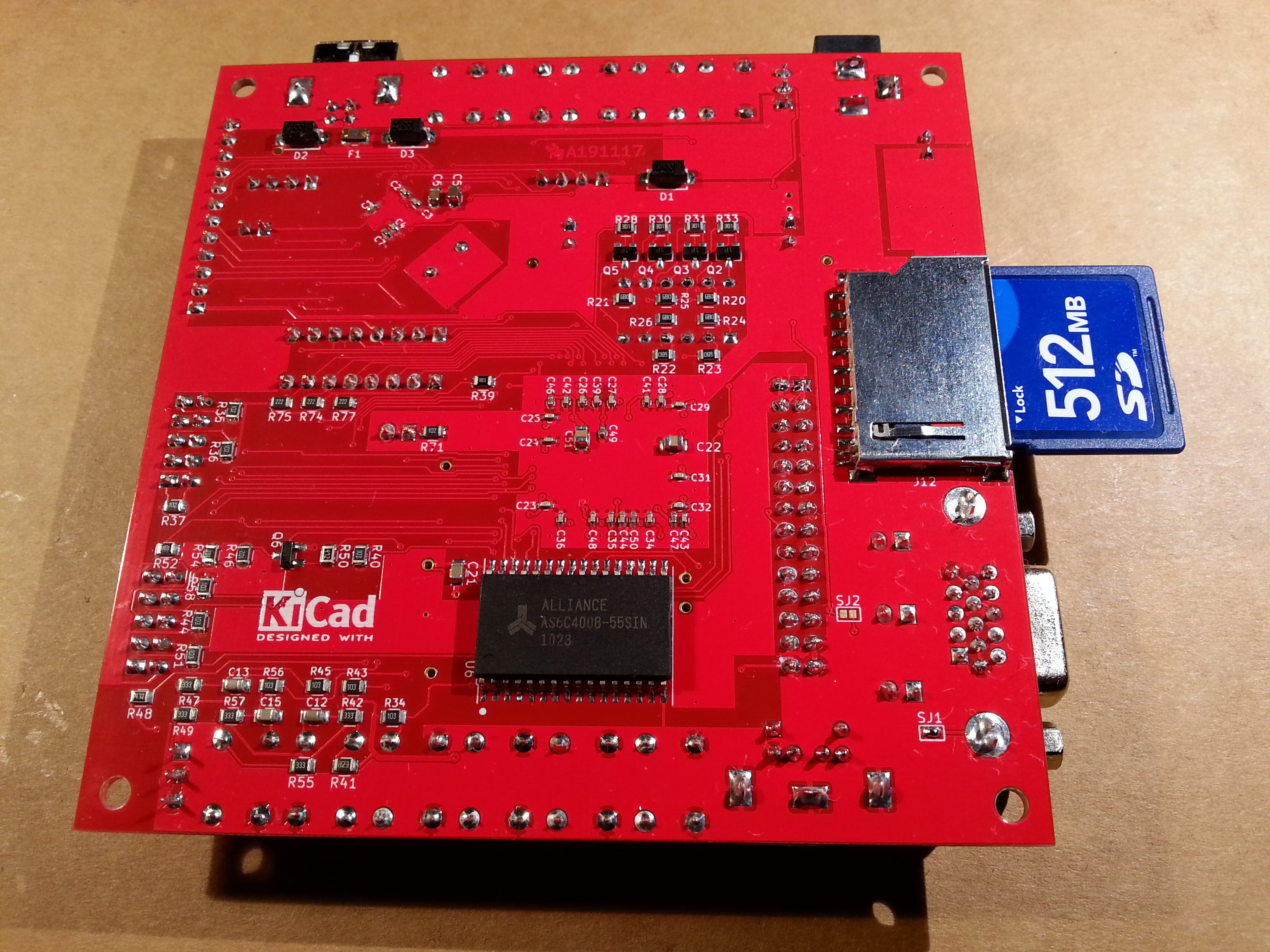
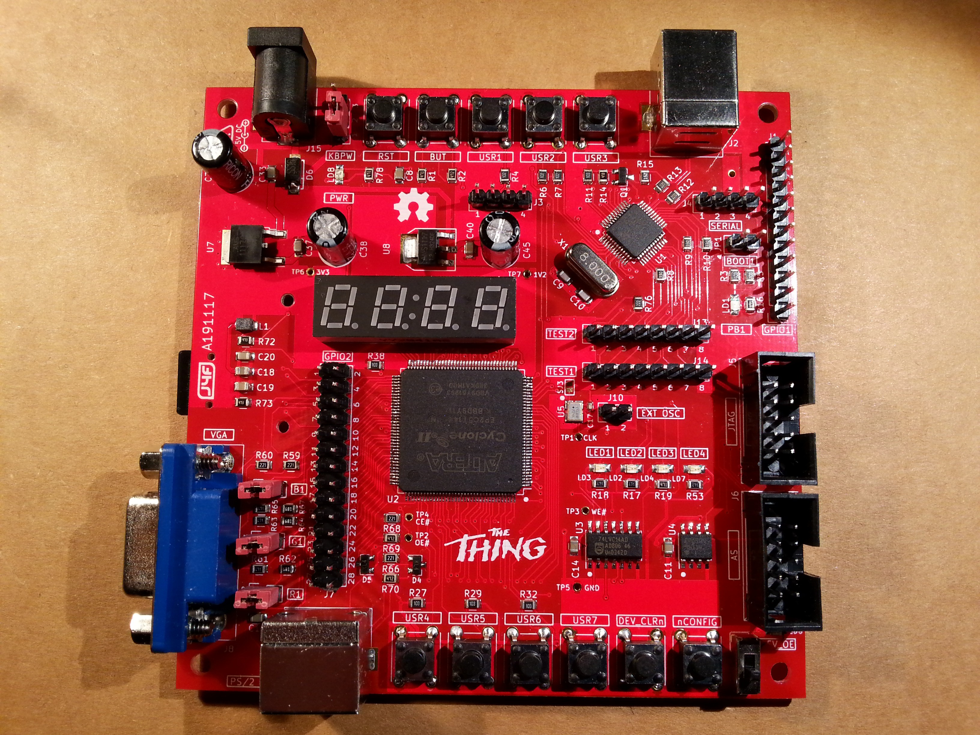
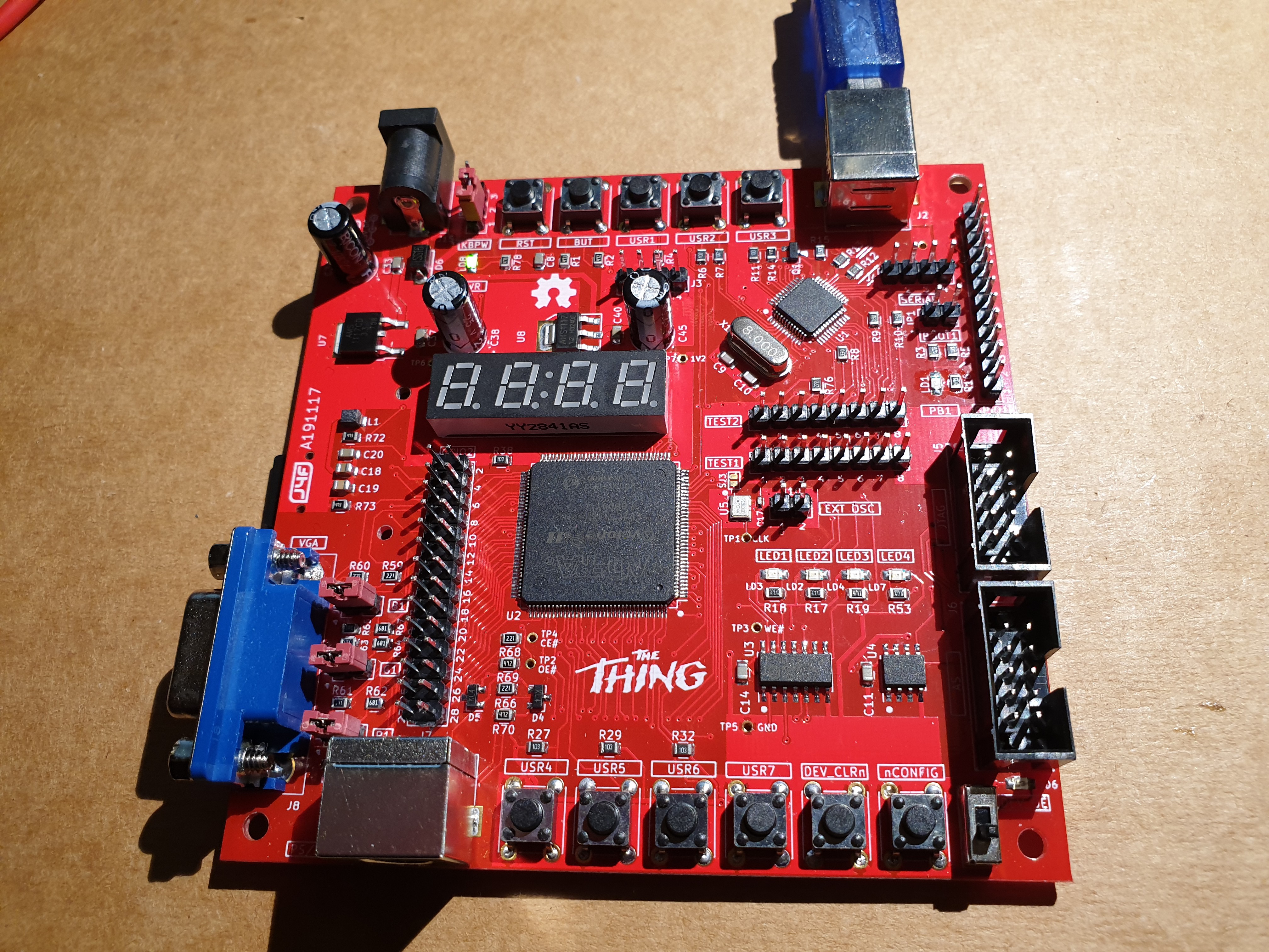
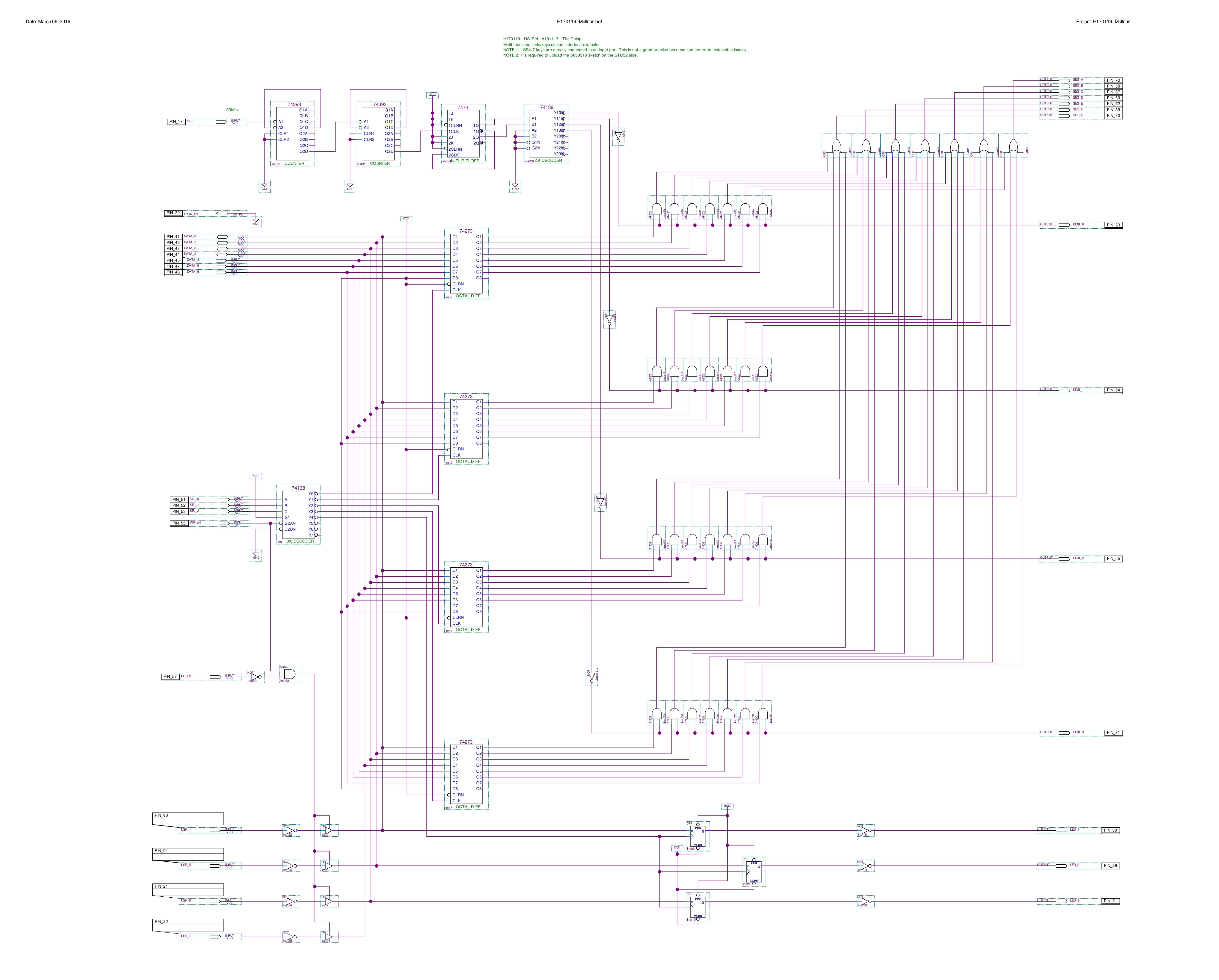
The Thing is the the "natural" evolution of the CPLD Fun Board. The idea was to make a FPGA board using cheap and easy to find components, with a STM32 Arduino used as "stimulus generator" or "companion" processor for the FPGA, and with a 512KB SRAM and common I/O as GPIOs, VGA and a PS/2 keyboard to "run" HDL SOCs.
More, it has the option to "run" easily Multicomp VHDL SOCs having the needed HW.
Multicomp is a modular VHDL design to "run" some famous retro 8 bit CPUs made by Grant Searle and described here.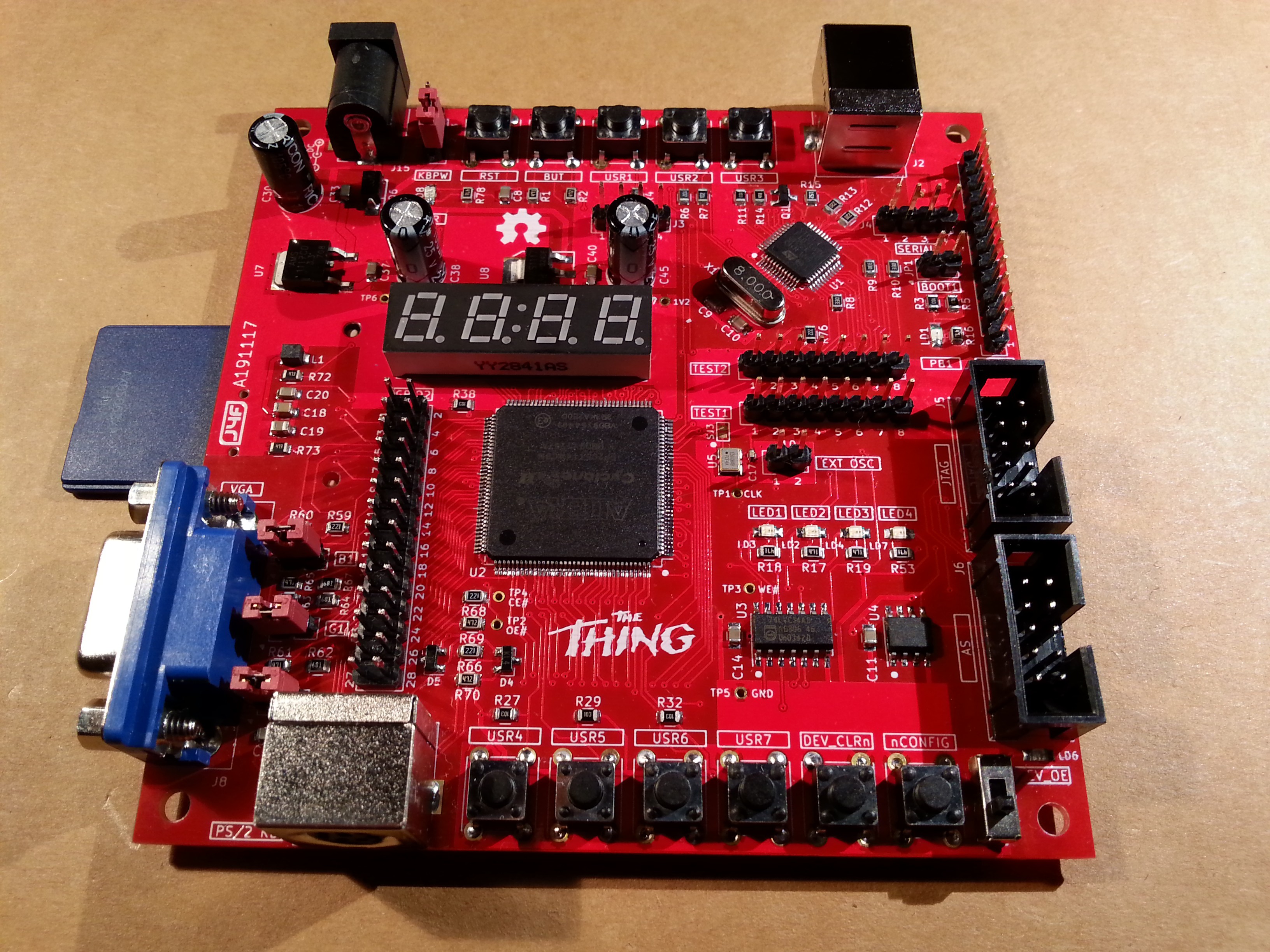
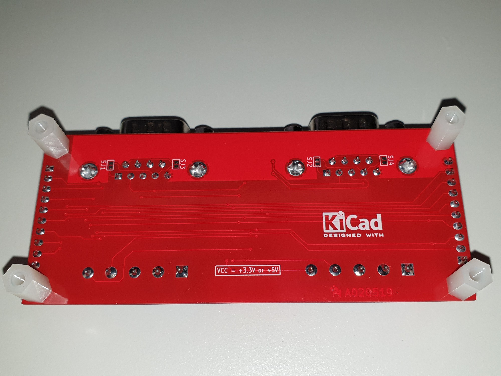
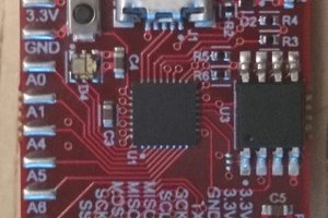
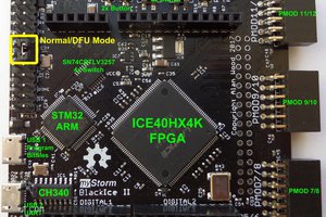
Here the details of the PCB. Please note that the PCB in the following image has an ENIG surface finish. This is not absolutely required. You can use a cheapest HASL surface finish:
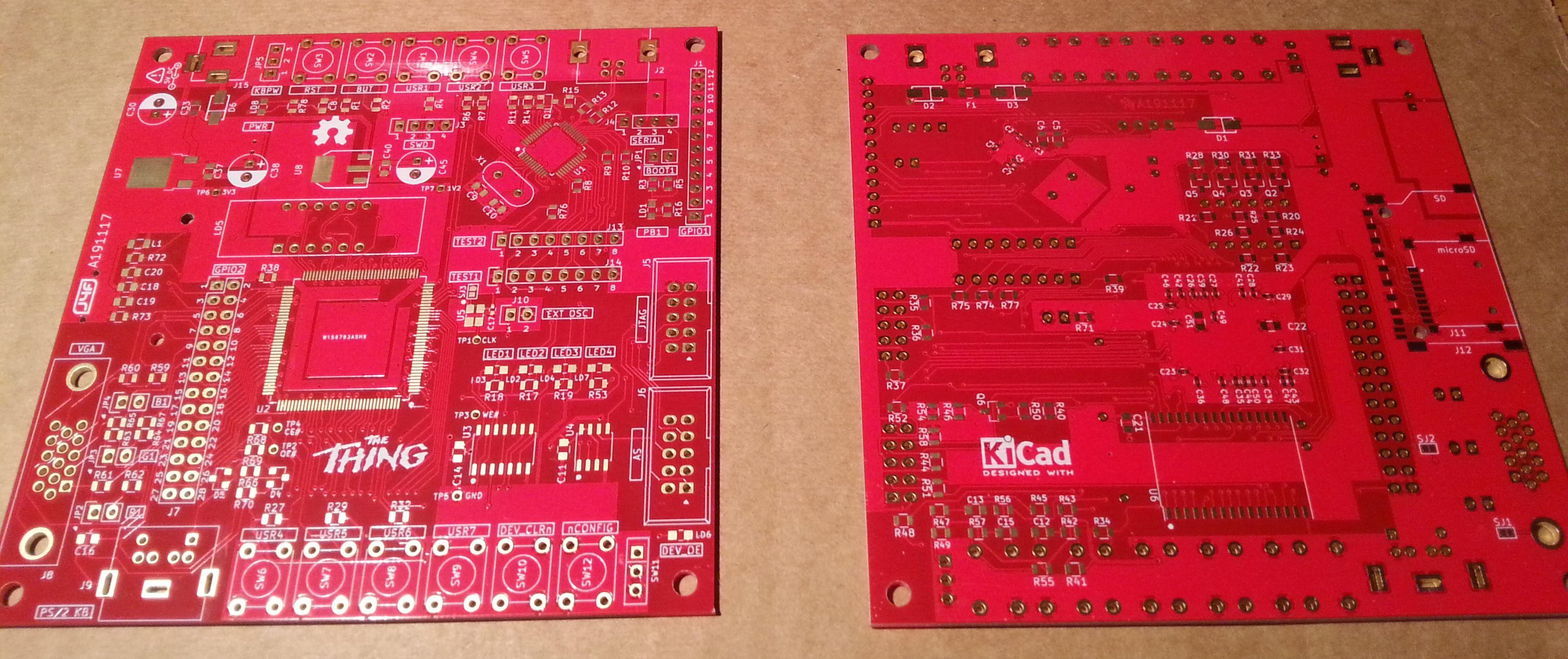
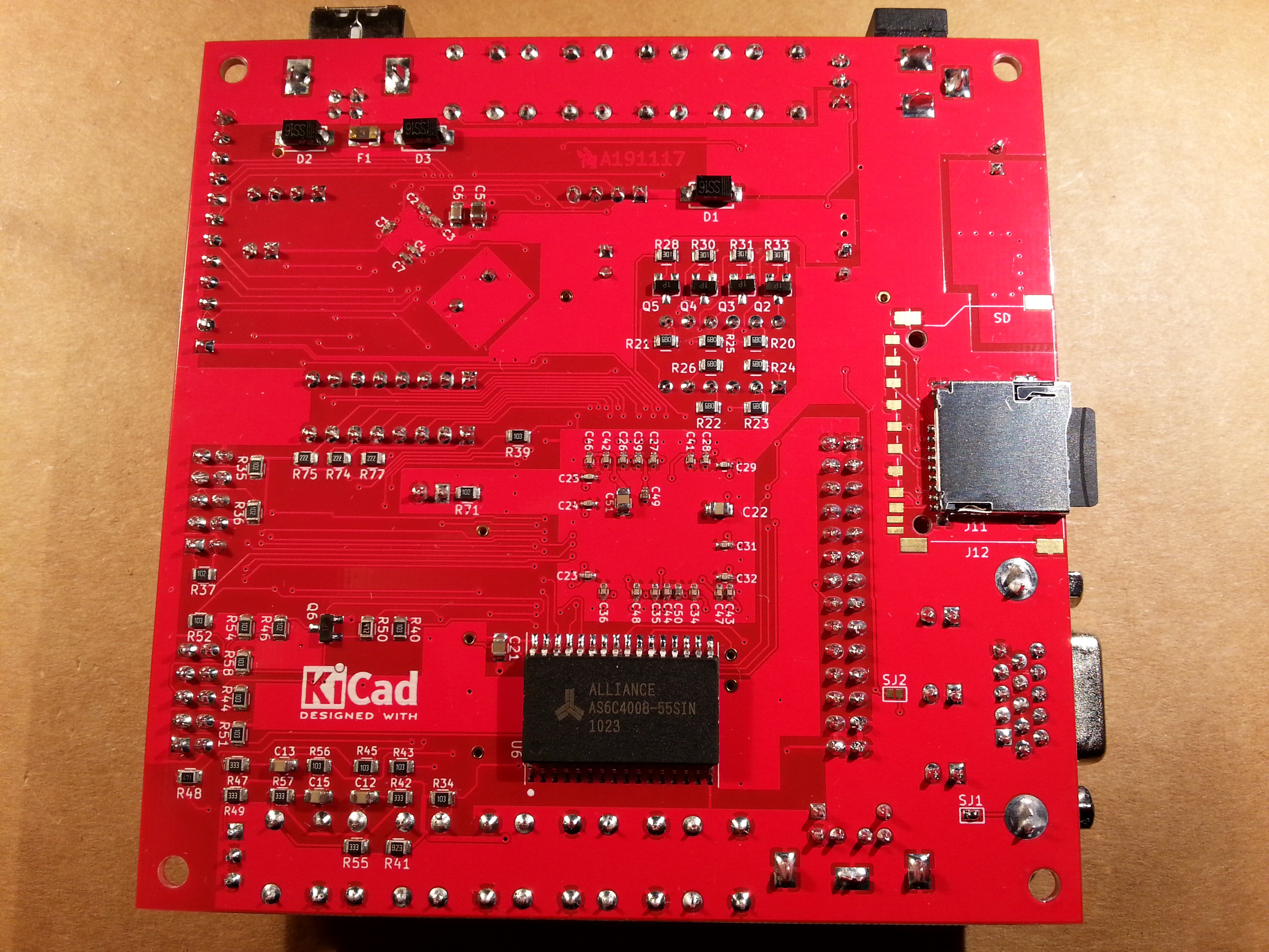
The PCB leaves the choice to solder a "legacy" SD socket (as in the previous images) or a micro-SD socket as shown in the following images:
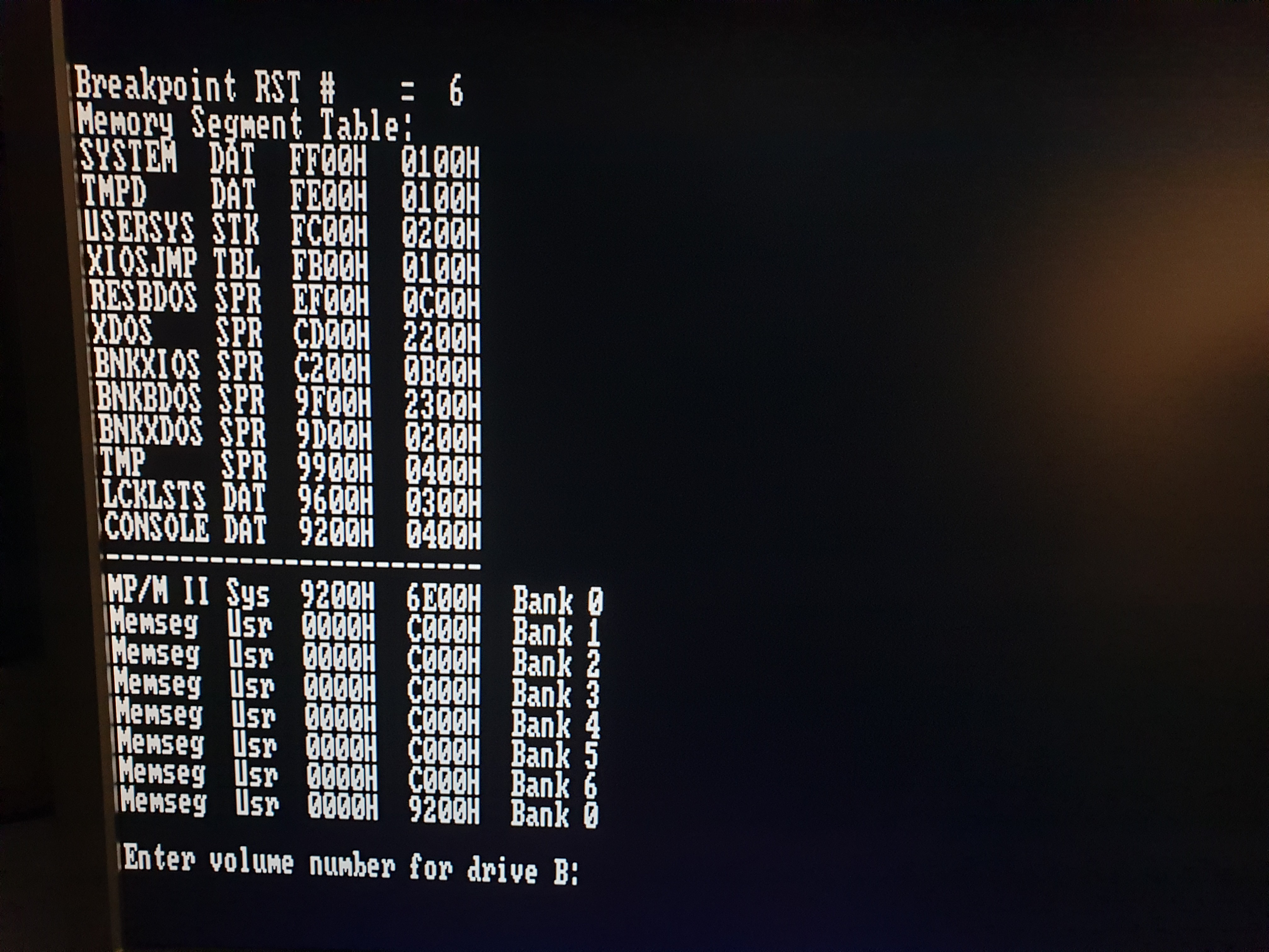
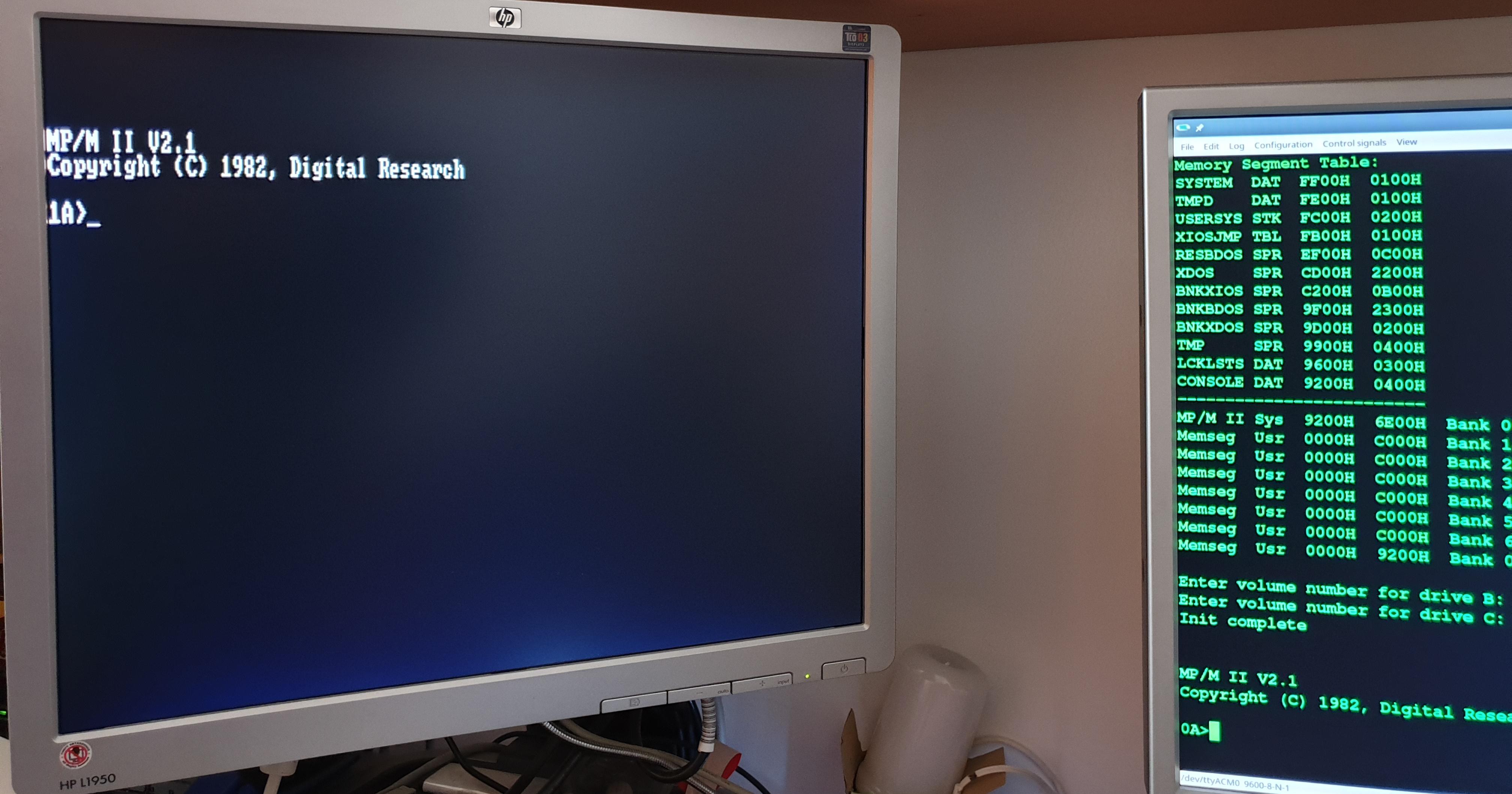
Here The Thing in action "running" a Multicomp Z80 with CP/M 2.2 as OS:
THE STM32 ARDUINO
The STM32F103C8T6 MCU is used as "stimulus generator" or "companion" MCU for the FPGA, and is easily programmed using the friendly Arduino IDE through the USB connector.
Five push buttons (RST, BUT, USER1-USER3) and a led (PB1) are reserved to the MCU.
There is also a dedicated GPIO connector (GPIO1).
The STM32F103 MCU side is "Maple Mini" compatible, so it possible to use the STM32F103 Arduino core provided by http://www.stm32duino.com (more info here). For a short story about the Maple Mini and the stm32duino see here.
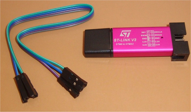
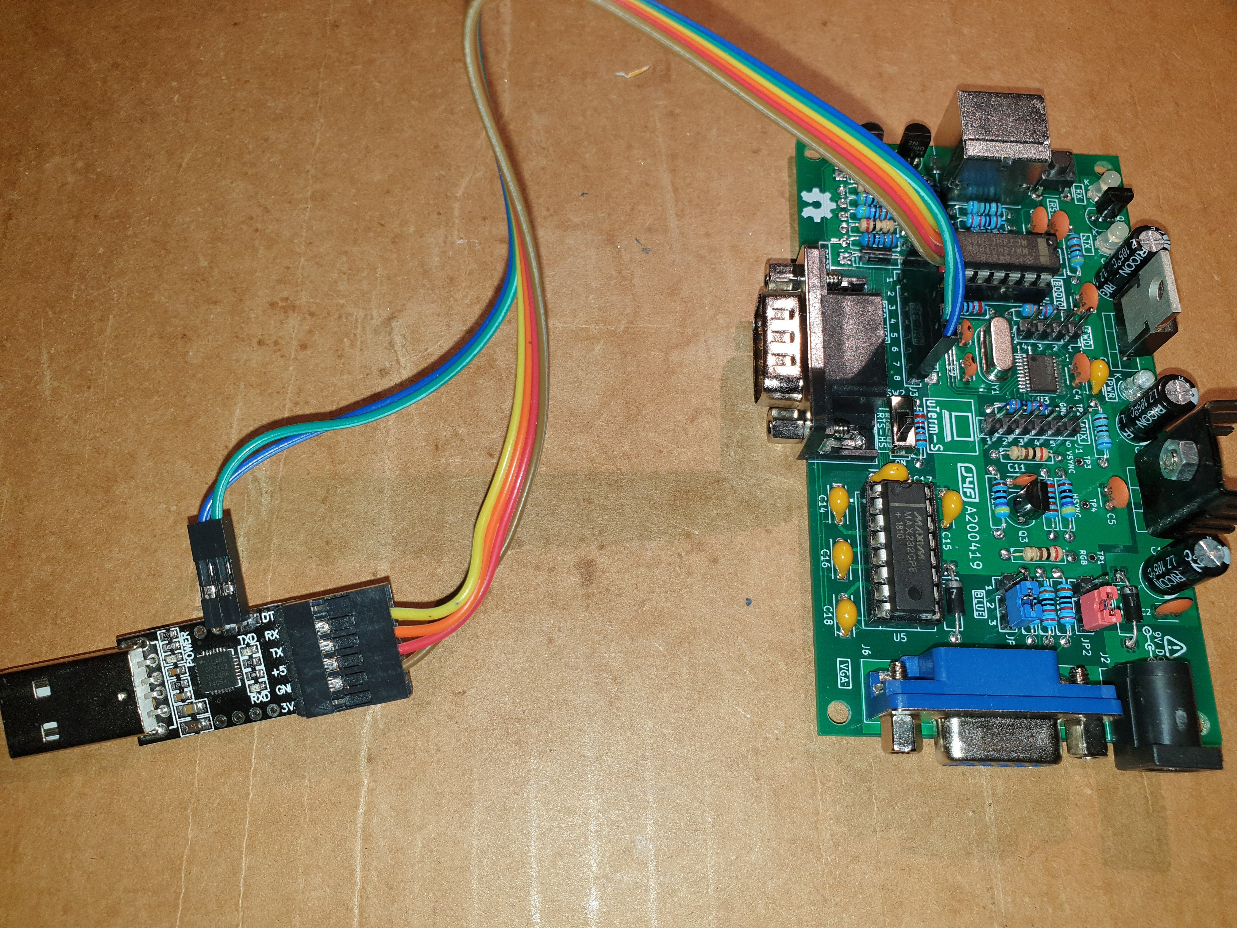
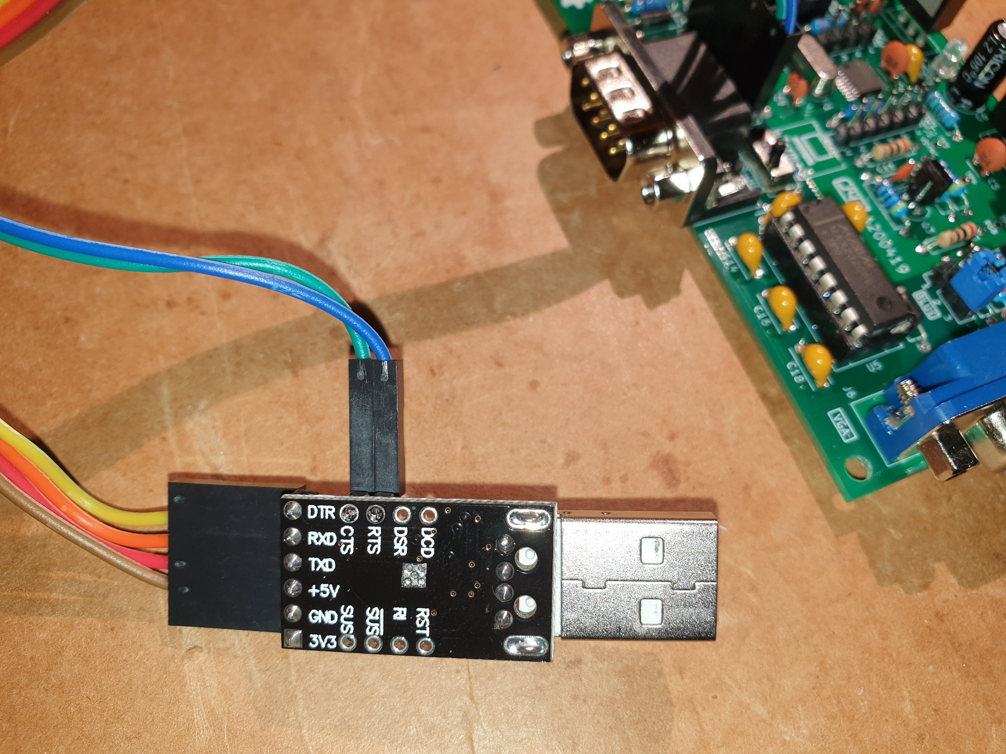
You need to flash the bootloader first using a cheap "St-Link V2" dongle through the SWD connector (or using a serial-USB adapter on the SERIAL connector. More info here).
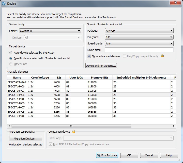
THE CYCLONE II FPGA
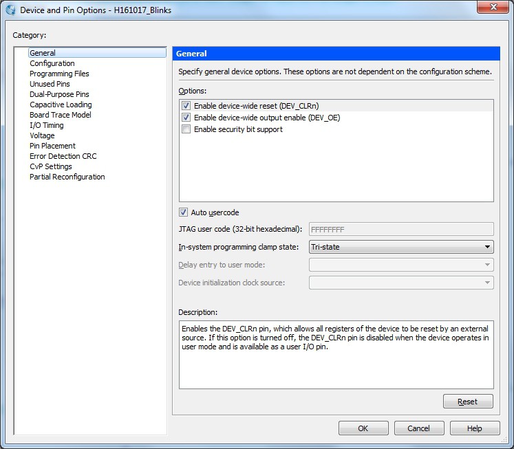
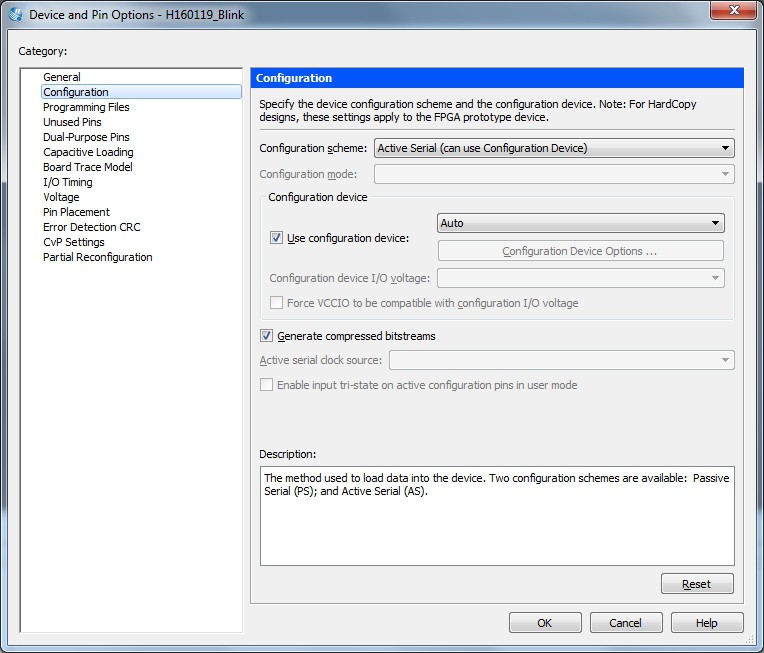
To configure the FPGA (EP2C5T144C8N) it is used the Quartus II IDE (the v13sp1 free edition is the last one supporting the Cyclone II FPGA) and a cheap "USB Blaster" dongle through the JTAG or AS connector.
To permanently store the FPGA configuration into the eeprom you can use the AS connector or also the JTAG connector with the SFL IP core as well explained in this Intel video.
... Read more »


 greg
greg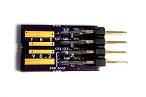
 ajlitt
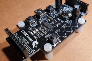
Thanks for this. Very cool design. Successfully built this over the holiday week. Flashed the bootloader into the STM32 and got your MultiFun demo working. Now to see what else I can get it to do.