 Just4Fun
This is a ready to use example of a custom "multi-functional" controller for a 4 digits 7-segments led display (single segment "graphic" drive mode with digits multiplexing), plus 3 status leds, plus 3 push buttons, using a bidirectional data bus (DATA_0-7) and a register selection bus (SEL_0-2). The command signals are an active low write signal (WR_EN) and an active low read signal (RD_EN). The behavior is very similar to a SRAM device.
To make things easier, in this example it is used the schematic editor and the 7400 devices family library, but note that this is not the best way to use a FPGA (the "right way" is to use VHDL/Verilog languages...).
The schematic is the following (this is an Hi-Res image. You can also use the Quartus II schematic editor to view it, opening the project):
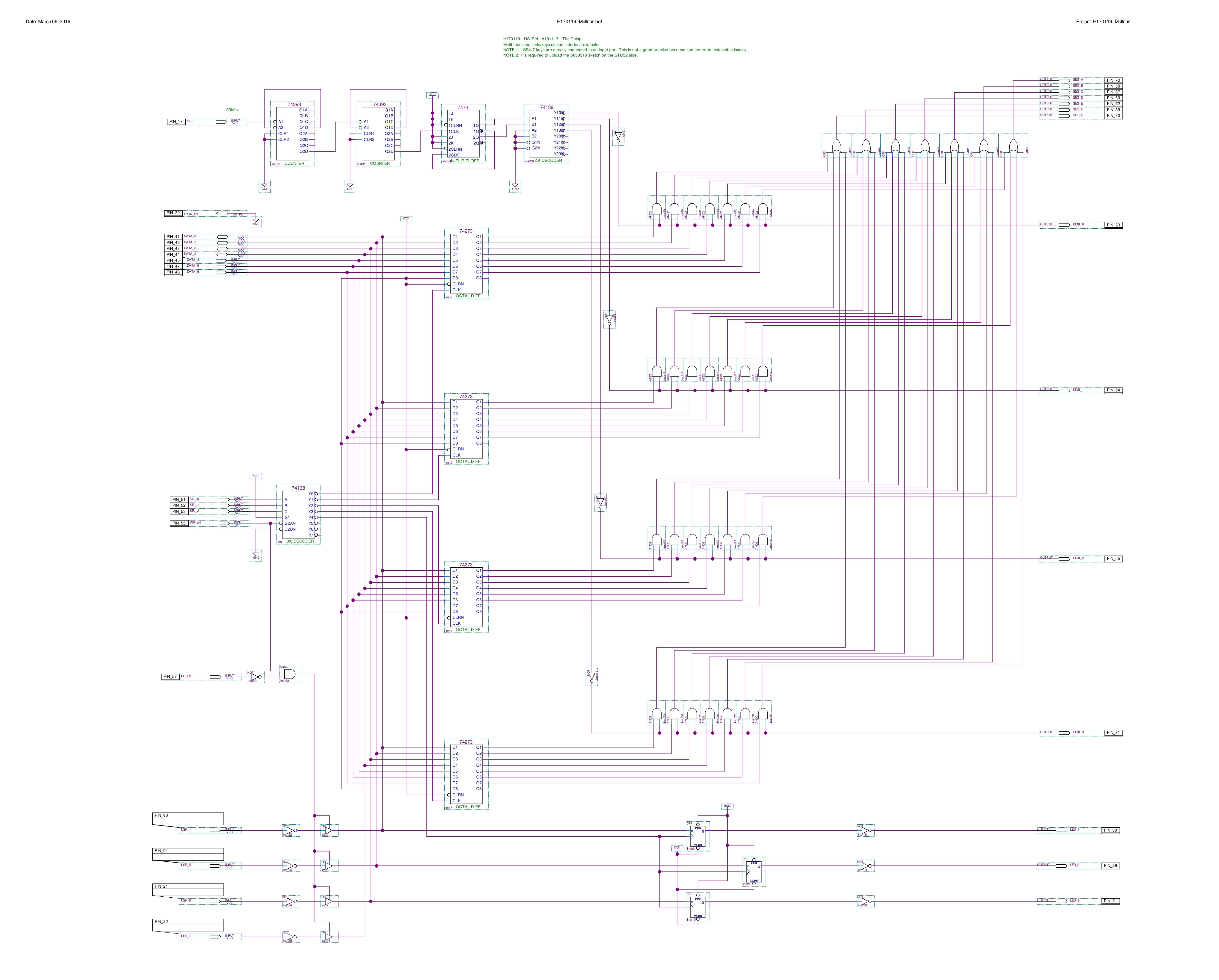
The input clock for the multiplex comes from the 50MHz oscillator, and is divided by two 1:256 dividers (74393).
The internal digit registers are 8 bits wide, because each single segment can be controlled, and there is a 3 bits register for the three leds LED1-3 (LED4 is a status led and isn't user "addressable").
Only DATA_0-3 lines are really bidirectional, DATA_4-7 lines are not used in "read" mode and are tied to "1" using internal pull-up resistors.
A logic "1" in the DATA bits means "led turned on" or "push button pressed".
In the "read" mode there is no real register involved, so the SEL_0-2 lines are all "don't care".
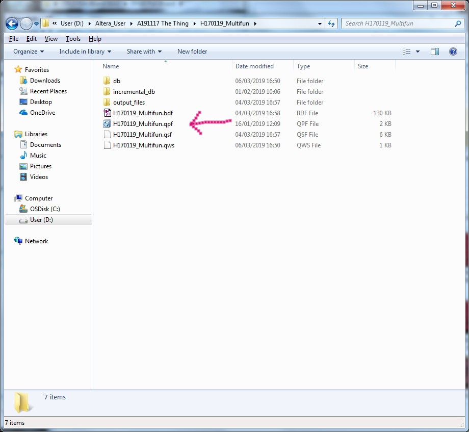
The complete Quartus II project (H170119_Multifun.zip) can be downloaded from the repository.
Unzip it taking its directory structure, and open it from the main Quartus II menu with "File" -> "Open Project..." selecting the file .qpf (is the extension for the Quartus II projects):
Upload the configuration into the FPGA using the JTAG connector, or with the AS connector to store it in the eeprom.
WARNING: Because this is a bidirectional interface, take in account the considerations done in the "The DEV_OE switch and led" Log.
The sketch for the MCU side (S030319_MultiFun.ino) can be downloaded from the repository.
The result is shown in this short video:
Note that the USR1-3 and BUT buttons are managed directly by the MCU (see the A191117 schematic). At the end of the video it is possible see the effect of the DEV_CLRn button (clears all the FFs inside the FPGA) and the DEV_OE switch (forces all the I/O pins of the FPGA in HiZ). The effect here is "visually" the same, but the inner behavior is different.
Discussions
Become a Hackaday.io Member
Create an account to leave a comment. Already have an account? Log In.