 Tony Robinson
The description below is now outdated, but if you like it read where I'm at now at https://tonyrobinson.com/dippy
Q: What do you mean by Acoustic Tubes? A: 40kHz ultrasonic transducers at each end of a 50cm to 1m plastic tube (air filled). The transmitter blasts out about 8 pulses at 40kHz and some time later they get picked up at the receiver. It's a mercury delay line without mercury. If you just pick the signal up at the reciever and send it back in, then the same signal should circulate forever, but if you pass it through an ALU then it stores the new values.
Q: What you mean by DIP switch ROM? A: Imagine an 8:256 address decoder, then any 8 bit address could result in a +ve signal to the top of an 8 way dip switch (and a LED lighting to tell you which DIP switch was used). The state of the 8 switches would dictate what signal ended up on the data bus.
Q: What do you mean by registers/RAM? To be honest I haven't worked out the correct term here. The CPU will have a program counter, but the registers/RAM will only be accessed by a data and return stack. The data stack starts at the bottom and grows upwards, the return stack starts at the top and grows downwards. There's no way to access any particular location directly, so RAM seems like the wrong term. But it's a stack, so registers seem like the wrong term as well.
Q: So what real registers exist? There will be a Program Counter (PC) and the Instruction that is being executed, both the full 8 bits. In addition there is a Data stack Pointer (DP) and a Return stack Pointer (RP). I'm undecided if DP and RP are 4 bit binary or 16 bit unary, the latter avoids having a dedicated INC/DEC for each and the 4:16 decoders, so 16 bit unary is probably the way to go.
Q: Will there be LEDs A: Oh yes, lots!
Q: Why, it can't run slow enough to see it working? A: Because it has to complete a clock cycle in the time it takes sound to get from one end to another. Ah, but maybe I can get a fast camera and show the result slowed down. Or use hardware to insert NOPs....
Q: So what do you think the instruction set will look like? A: something like this:
NOP No operation
PUSH DATA This pushes the byte following the PUSH instruction onto the data stack (and so increments the data pointer). This is the only two byte instruction.
IN takes a byte from a preloaded LED array and pushes it to the top of data stack.
OUT This pulls the top of the data stack and writes it to the LED display as a shift register.
JSR ADDR jump to subroutine at the address following the JSR code. This pushes the PC+1 onto the return stack. Note that all other instructions have the bottom bit set and if the bottom bit is clear then it's a JSR ADDR (and ADDR is even).
RET pop the return stack
D2R/R2D pop data stack and push on return stack (and vice versa). Forth uses >r, r> and r@.
DROP decrement the data stack pointer so discarding the top element
SWAP swap the top two elements on the data stack
NOT/INC/DEC - ALU instructions on the top element of the data stack
AND/OR/XOR/ADD/SUB/ADDc/SUBc - ALU instructions that read the top two elements and write one back to the data stack.
I'm undecided as to whether there should be a carry flag (that's ADDc, SUBc), as there isn't the space to have big numbers.
I like non-destructive operations, so may have nAND that leaves the two operands on the data stack and pushes the result.
Operations set two Boolean flags, one is ZERO, which is only set if all the bits were zero, the...
Read more »


 jaromir.sukuba
 Артём Шакиров
 Szoftveres
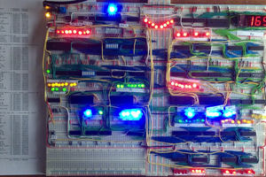
 James Bates
That video @matseng linked to is interesting. If I understand correctly, the number of bits that can be stored by the delay line is related to the distance between mic and speaker. Is that correct? If so, I wonder if using something other than air as your conducting medium will either allow you to physically shorten the delay line or increase the number of bits for the same length. Maybe sulfur hexafluoride?