 Alastair Hewitt
The redesign is complete and everything has changed. I'll need to go back and update all the logs because most of that information is no longer valid. Things have been rationalized and the timing simplified. This has resulted in an even faster machine that could potentially run on the higher VESA dot clock of 31.5 MHz. More on that after some more testing.
The big change was getting rid of the clock and strobe timing. The clocks control the bus context and the strobes were used to latch data within the bus timing. A strobe would be 6ns before the end of the bus cycle to allow time to hold the latched data before the context switch.
This wasn't needed though because the ROM owns its data bus. Data from the previous context can be left on the bus after the switch from the GPU to CPU. The bus tri-state takes at least 3ns to change the address and the ROM is guaranteed to hold the data for at least 7ns after that. Since the data will stick around on the bus for at least 10ns then the same clock used for the bus control can be used to latch the data, even after one-layer of logic delay. This effectively overlaps the clock cycles and time can be borrowed from the next cycle to extend the previous one.
The build is finally starting to take shape. Things are progressing slowly since everything is being validated at every step. Bus contention is also being checked and one issue was resolved that would happen on reset. The new clock circuit needs to be reset to synchronize two independent ring counters. If the clocks are all pulled low then both bus contexts exist at the same time. This effectively shorts any TTL output that is driving a high on to the same bus line as something holding it low. The new circuit uses flip-flops with complementary outputs to prevent this.
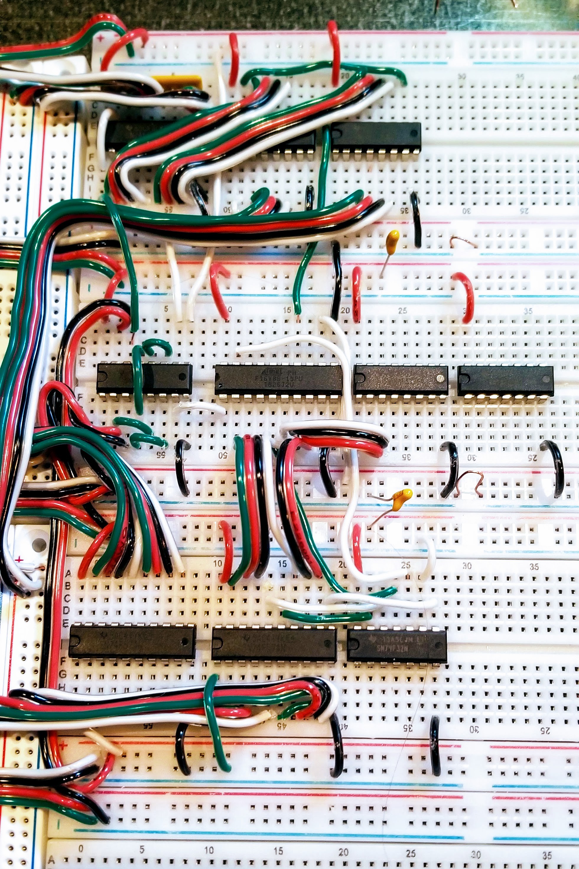
The picture below shows the bare-bones CPU (ROM not shown). This contains the main clock generator, CPU state machine, Program Counter and bus buffer, Instruction register, and a little bit of logic (not all wired up in this picture). There's also an additional register to drive something on the bus during the GPU bus cycle.
The ROM was programmed with sequential groups of 16 instructions. The instruction sequences demonstrate different execution cycles. The oscilloscope output below shows the least significant bit of the Program Counter. Going from left to right you can see cycles where the PC is incremented every 4 machine cycles, then every 6, every 2, and then every 1 cycle before going back to 2, then 4.
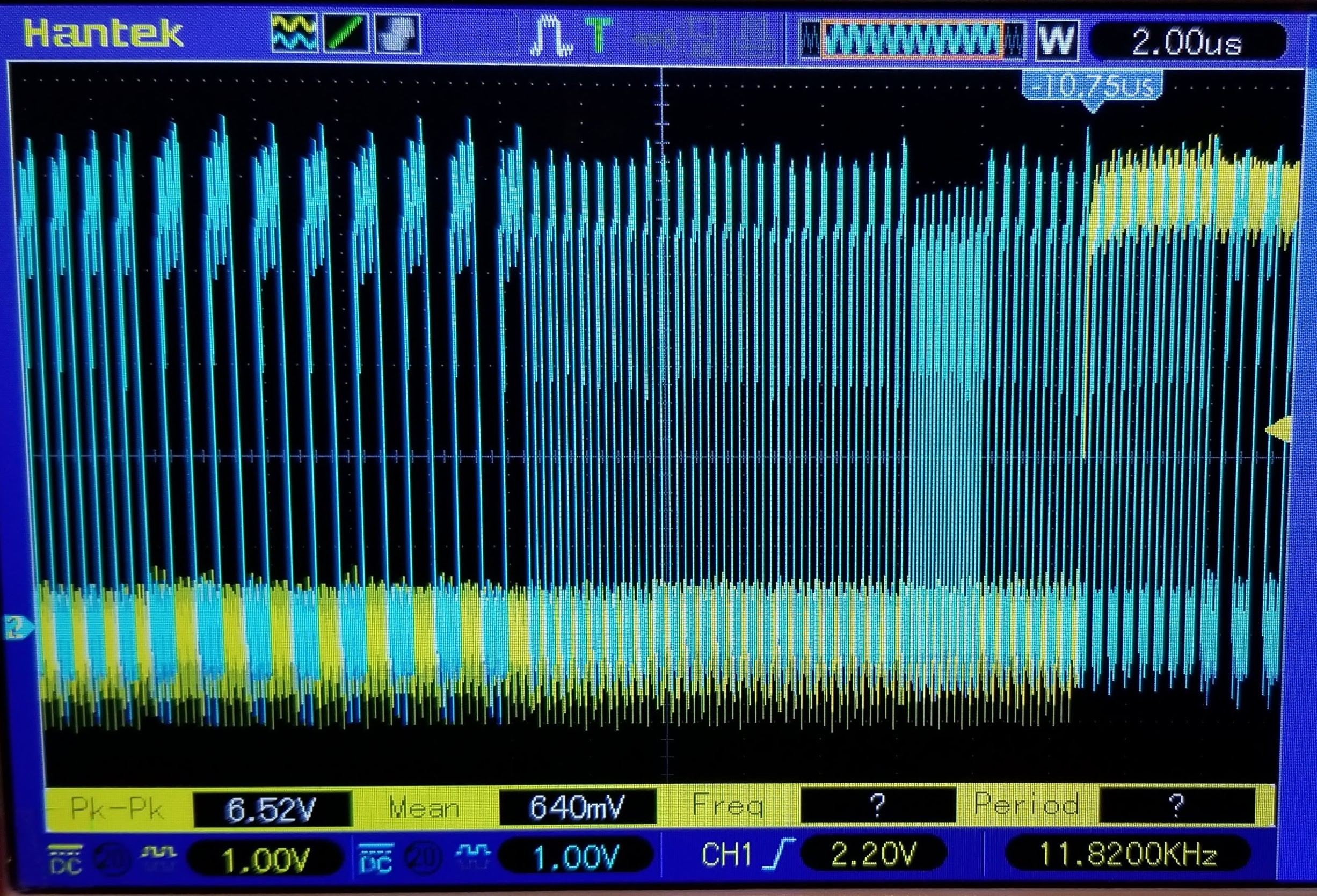
The instructions executed above are:
- Short ALU - 4 cycles between PC increments
- Long ALU - 6 cycles between PC increments
- Load Zero-page - 2 cycles between PC increments
- Load Operand - 2 cycles between PC increments
- Page Jump (unconditional) - 2 cycles between PC increments
- Jump (condition not met) - 1 cycle PC increment
- Jump (unconditional) - 2 cycles between PC increments
- NOP - 2 cycles between PC increments
Next up is a jump program that will reload the Program Counter and execute a loop. Then add the accumulator and program some ALU functions.
Discussions
Become a Hackaday.io Member
Create an account to leave a comment. Already have an account? Log In.