 Alastair Hewitt
The redesign continued to ECU section. The changes are fairly significant, so much so that the breadboard build needs to start over. It was almost back to the drawing board, but the CPU section remains fairly intact. The result is another reduction in chip count to bring the TTL count down to 37 chips.
The original design packed the instructions into just 8-bits. The instructions need to define the instruction type, ALU function, data source, and destination register. The original encoding resulted in a lot of limitations in the available instructions to pack so much into so little space.
The instructions do provide everything needed to write code, but actual programs were quickly exposing the instruction set limitations. Quite often additional instructions are needed to move the result from the ALU to the desired register. There is no specific move instruction, so this requires the ALU identity function to target the final register. This results in a lot of wasted cycles.
The solution is to expand the size of the instructions. The ROM is still 8-bits wide, so this requires an additional cycle to load another byte to get to 16 bits. However, one bit of the first instruction byte can be used to tell the state machine if a second instruction byte should be loaded. This allows variable-length instructions, with a limited set of 7-bit instructions and a full set of 16-bit instructions.
The new design is using instructions of this format:
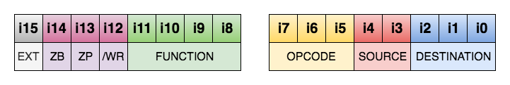
Destination is one of the 8 possible registers (Pg, PC, SC, V, HL, E, X, Y). Source is one of 4 data sources (A, X, E, RAM). There are 8 possible opcodes, with the following 6 defined:
- LD - load operand (source not used)
- LDC - load conditional (source defines condition)
- MV - move source to destination
- FNH - ALU unary function defined by H - destination = FNH(source)
- FN4 - nibble-wide ALU binary function
- FN8 - byte-wide ALU binary function
The first 4 opcodes define 7-bit instructions. The most-significant bit of these is high and this stops the state machine from loading the second byte. The most-significant bit is also the output enable (active low) of the second instruction register, so the second register is tri-stated and the value pulled high to 0xFF. The ALU binary functions require all 16-bits, so the most-significant bit of the last two opcodes is low. Along with the 4-bit ALU function there are some additional bits as follows:
The /WE bit (active low) enables write enable on the RAM cycle and stores the result in memory. The ZP bit (active high) specifies the zero page when the RAM is addressed. In a similar way, the ZB bit (active high) specifies the zero bank (the memory bank that contains the display). The EXT bit (active low) specified a set of extended registers and will switch the destination from the internal 8 registers to 8 possible external registers.
The default values of the second instruction byte are therefore: internal registers, zero bank and page, memory read only, FNH ALU function. This means the RAM source comes from the zero page in the zero bank for the 7-bit instructions.
This instruction format now defines almost everything needed in a single instruction. This improves performance, even though some instructions require an additional cycle to load the second instruction byte. The new format is using about 60% of the cycles to run the same code. The simpler encoding also reduces the amount of logic in the ECU, so a net reduction in chips, even though a second instruction register was added.
Next up is a new schematic, complete redesign the PAL, and redo the entire breadboard... so basically, back to square one :(
Discussions
Become a Hackaday.io Member
Create an account to leave a comment. Already have an account? Log In.