 Ross Bamford
As I mentioned in the previous log, the revision zero PCBs arrived last week, and I finally had time to source the final few parts I was missing (a few IC sockets) and solder up the boards. I wanted to socket all the chips for this first population in order to have fewer variables when it came to checking if the board actually worked (i.e. it would eliminate the possibility of me blowing an IC through ham-fisted soldering - I've even socketed the 555!)
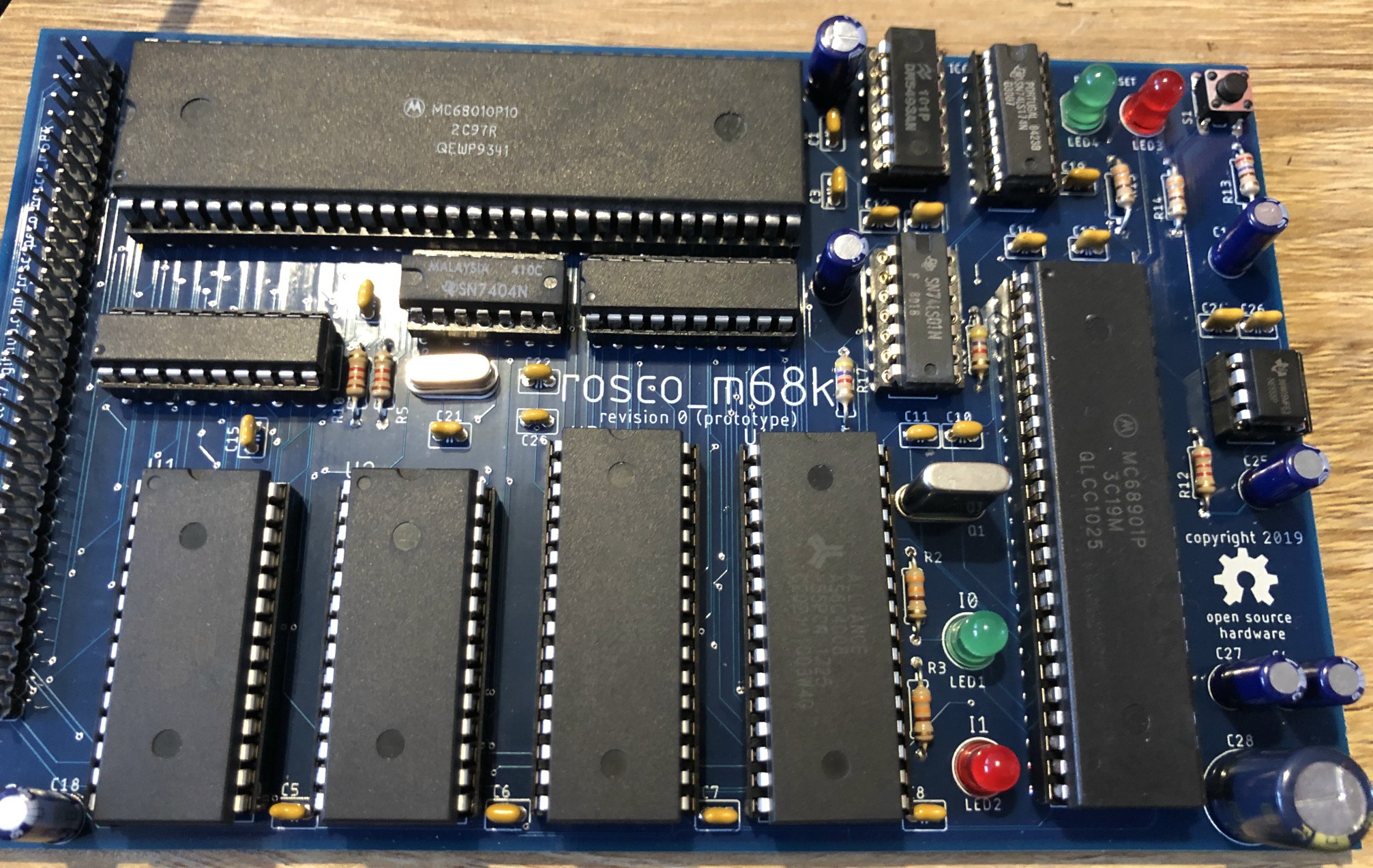
I'm pleased to say that, a few minor issues aside, the board works perfectly, and is happily running the same firmware and test code that runs on the breadboard. The PCBs from JLCPCB are fantastic and lead-free hand-soldering was a breeze, even with the small clearances on a few of the vias I talked about previously.
The finished board looks like this:
I still haven't been able to get hold of any 74LS93s (they're in-transit from China) so I've substituted with a DM5493 I picked up as surplus from a local electronics store, and of course it works fine.
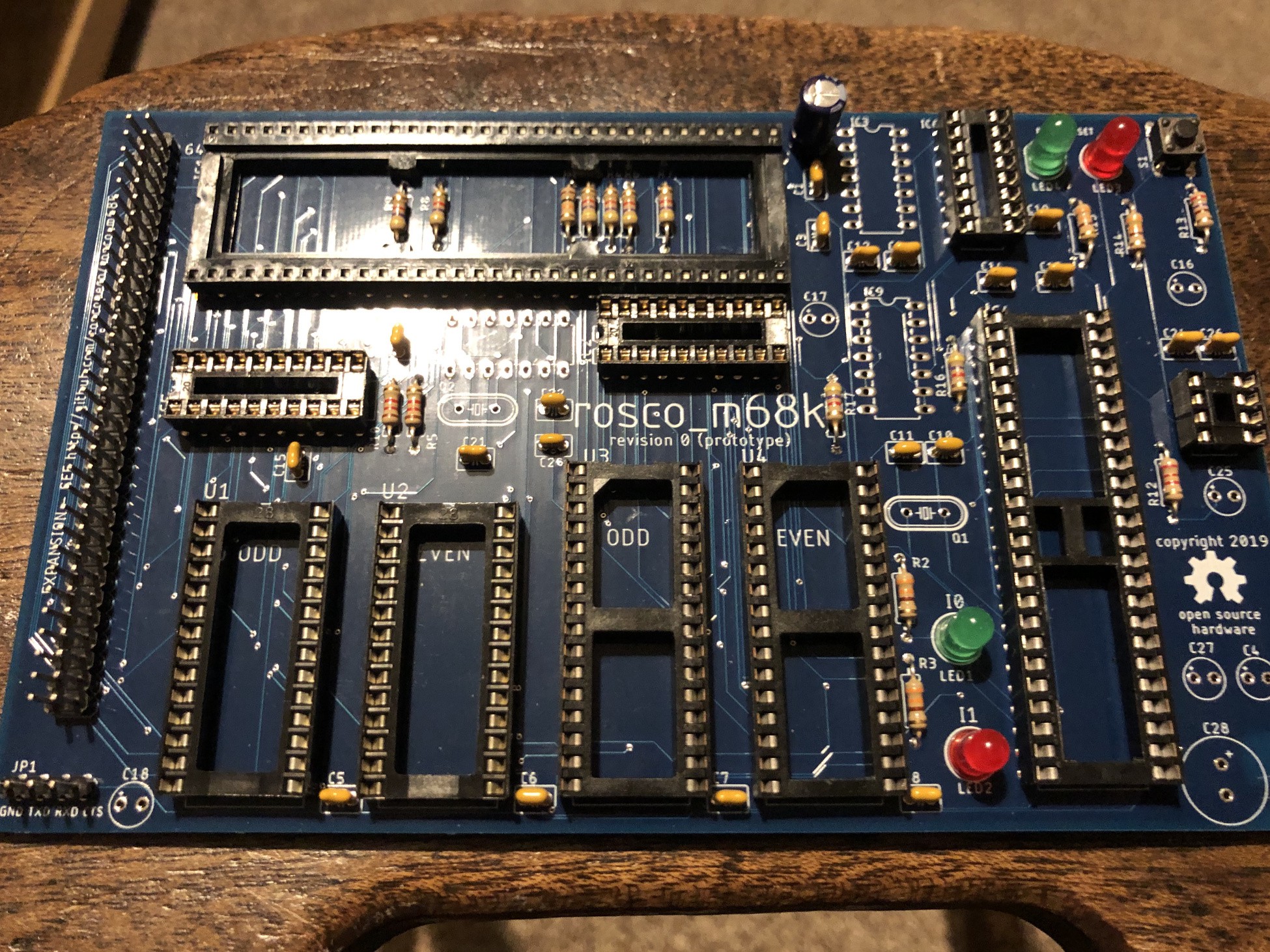
In terms of problems, there were two - one simple, and one slightly less so. The first is that, when I designed the board, I envisaged using 64-pin DIL sockets with a single brace (aside: is there an actual term for these things?) halfway along, but in reality I wasn't able to get such a thing, and instead got sockets with two braces, at 1/3 and 2/3 of the length. This wouldn't be a problem except for the fact I've stashed some pull-up resistors under the IC, and the placement of them was exactly wrong for this type of socket.
This wasn't a huge thing, I simply cut the braces out - once the socket is soldered it should be strong enough without them, as long as a bit of care is taken when inserting the chip. You can clearly see this hack before the chip is inserted (at the top of the image), but it's neatly hidden once the CPU is in place:
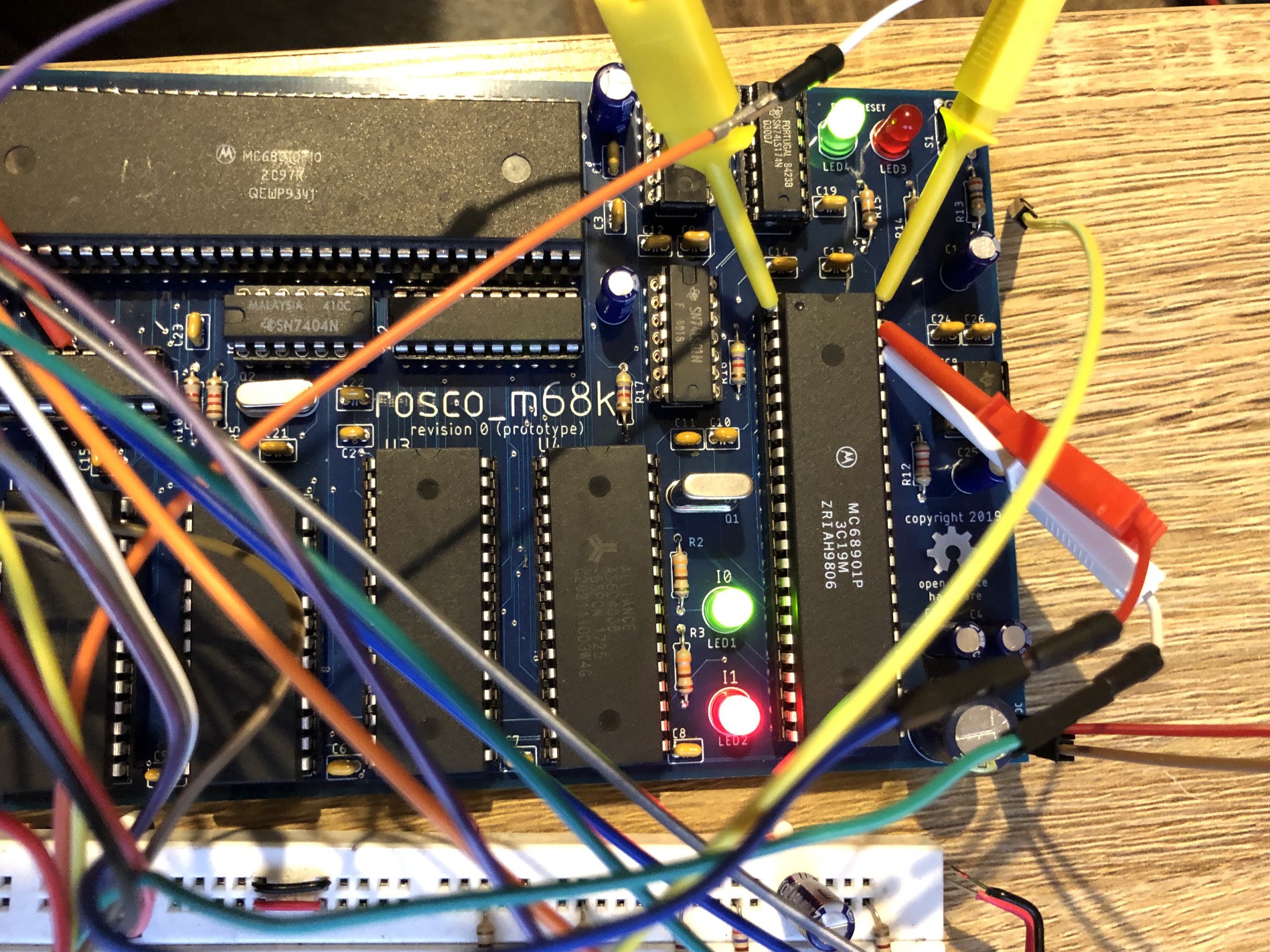
The second problem took a little debugging, but I finally figured it out in the small hours of Sunday morning. I had to hook up the logic analyser, and wire to the LED panel I used for the breadboard build so I could watch what the address decoder was doing:

By this point I'd narrowed down the problem to something 68901-related, as the traces from the CPU all seemed fine - it wasn't wandering off into random memory, or getting stuck waiting for DTACK - it was definitely working, I just wasn't sure on what as the serial output was dead and the two indicator LEDs weren't working at all.
Through some debugging of the MFP (basically making sure it was being selected, was generating its own DTACK signal properly, and that this was being treated correctly by the glue logic) I tracked the problem down to a silly mistake in the schematic:
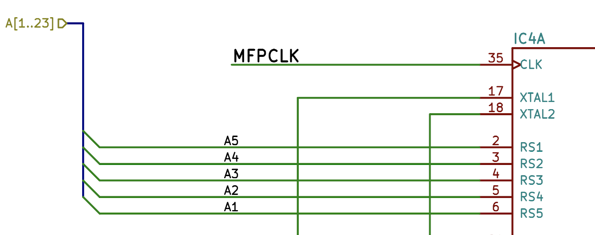
Yep - I've connected the register select lines of the 68901 to the address bus backwards... Cue massive facepalm, but happily this is an issue that can be worked around in software (by simply reversing the bits 1-5 in the MFP register addresses) so not a major problem. I raised a ticket to fix it properly, and did the workaround locally to continue with the testing.
With that done, the board is working perfectly, as can be seen from the two indicator LEDs in the image below - this is running some test code that lights I0 once the memory test is complete, then lights I1 and flashes it once the MFP is fully initialised and interrupts are enabled.
And just like that, the project's breadboard days are over! I'll miss the breadboard, and I feel kind-of bad about tearing it down, but I've already had to steal a few parts from it (due to ongoing shipping issues thanks in part to Coronavirus), and I definitely won't miss the occasional blips when it just stopped working due to loose connections etc.
Oh, and debugging is much more convenient with the smaller PCB and its expansion connector, too...
Discussions
Become a Hackaday.io Member
Create an account to leave a comment. Already have an account? Log In.
I'm really rather jealous that you've got to this stage so quickly! Out of interest, for the expansion port how do you plan to leverage that? Are you thinking of adding some kind of bus board that then has other ports on it? I'm assuming from the images it's made from standard pin headers? Maybe if I get my design going I could at least configure it to use the same expansion bus layout!
Are you sure? yes | no
Thanks, though it probably just means I have too much free time :D the expansion connector is mostly just for debugging in this iteration of the board but in the next revision I’m planning to maybe make it compatible with some kind of bus board, probably with some buffers and some protection diodes etc. It’s just standard pin headers, it would be awesome if yours was compatible, we could collaborate on expansions :) I’m planning to do graphics first but will be changing the connector on the next revision, removing some of the useless (as far as expansions are concerned) address decoder signals and replacing them with the legacy peripheral signals from the CPU. FWIW the current pinout of the connector is at https://github.com/roscopeco/rosco_m68k/blob/master/design/jp3_pinout.md (note there’s an error on the silkscreen which can confuse the pin numbering, https://github.com/roscopeco/rosco_m68k/issues/8
Are you sure? yes | no