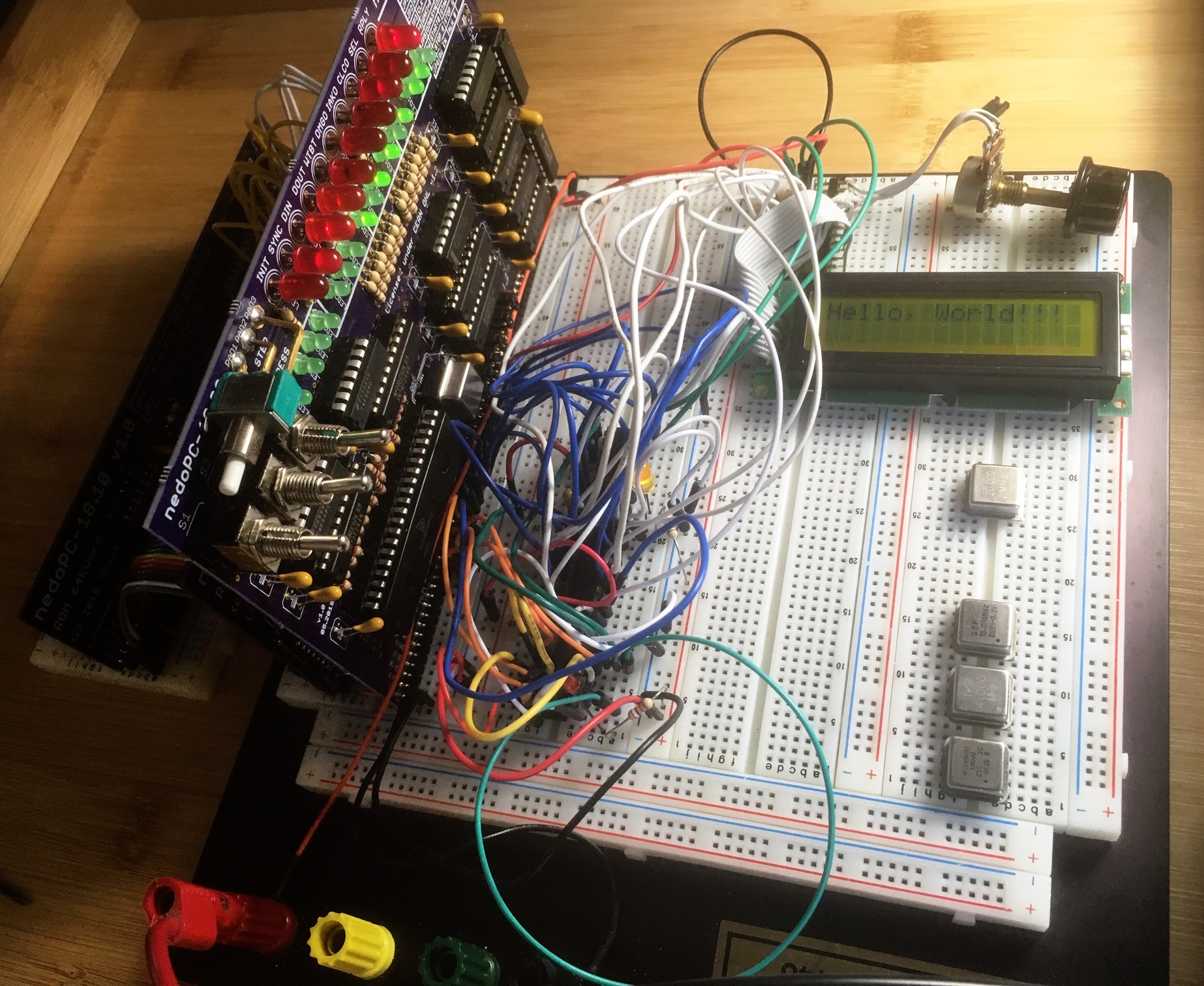
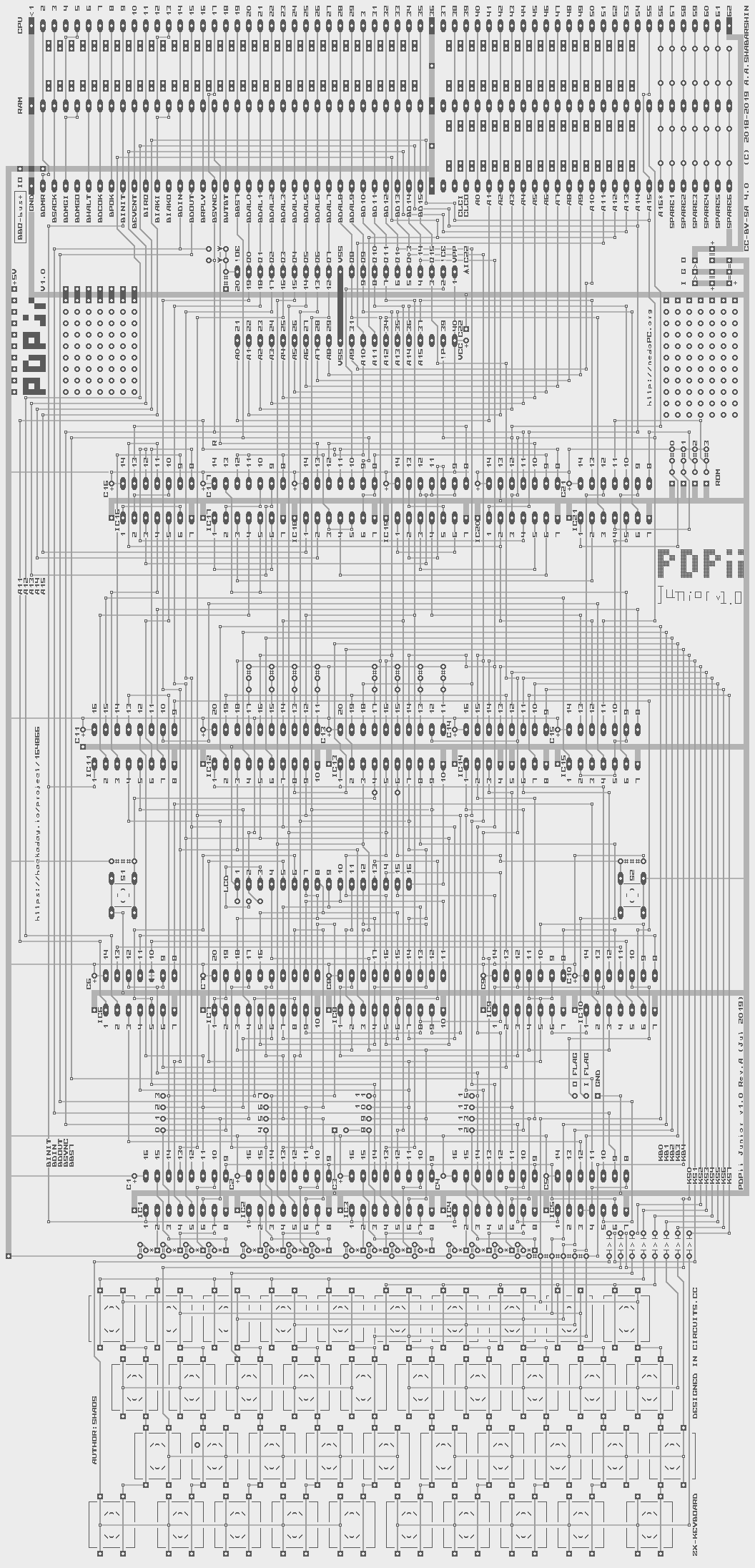
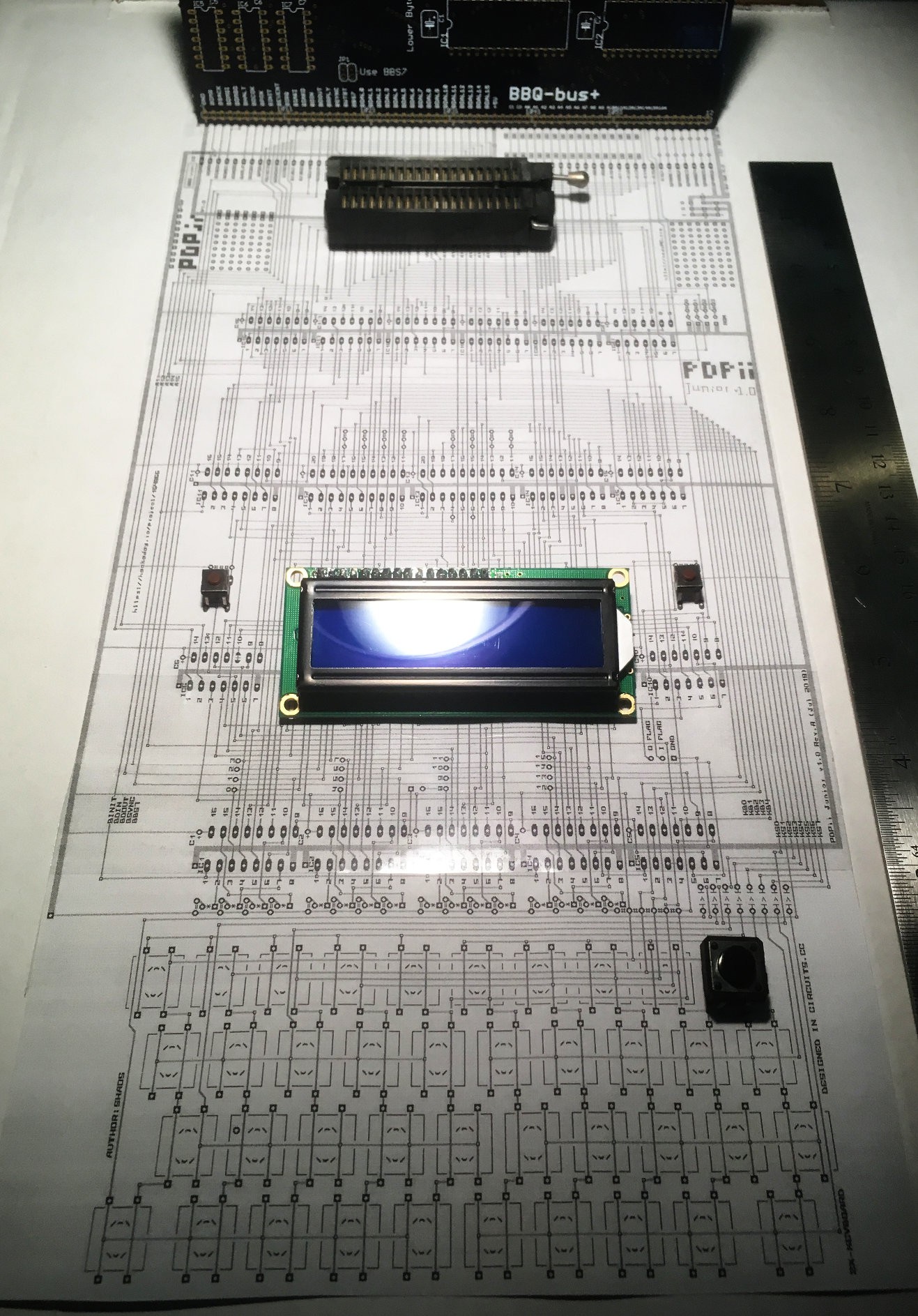
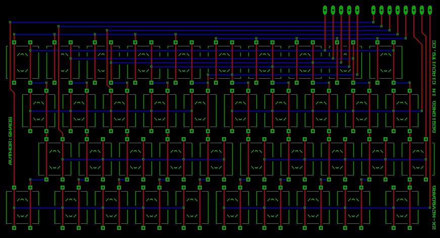
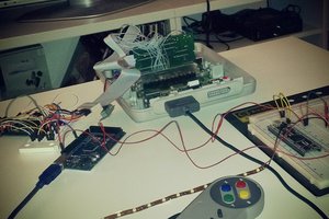
Close
0%
0%

PDPjr

Standalone DIY 16-bit computer "PDPii Junior"

Public Chat
Similar projects worth following
"Junior PDPii" is simplified #PDPii standalone DIY computer with 16x2 text LCD, 32KB RAM, 128KB ROM, Russian 16-bit CPU KR1801VM with PDP-11 instruction set and ZX-Spectrum keyboard (on the motherboard itself).

PDPii Junior is simplified #PDPii created specifically for Hackaday Prize 2019 in attempt to make a product. It will use CPU-module from #PDPii project with 1801VM2 (PDP-11 instruction set), #PDPii  16 KWords RAM module (in dedicated slot with slightly modified wiring to be able to mask RAM if needed) and also it will have 64 KWords ROM on-board (single chip 27C1024), 16x2 text LCD with parallel interface and on-board keyboard that is similar to ZX-Spectrum one (but it will be possible to connect any matrix keyboard with up to 104 buttons with help of 8 extra inputs). Current state:

Goal number 1 - run RT-11, stretch goal - run downsized Unix :)

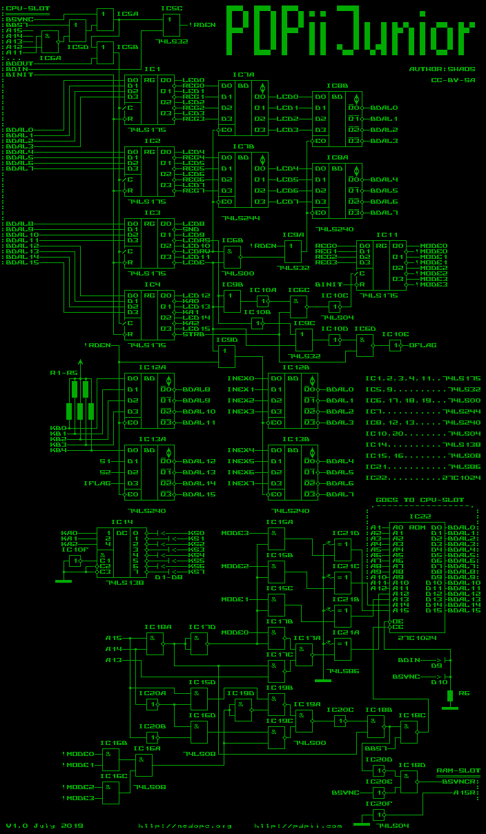
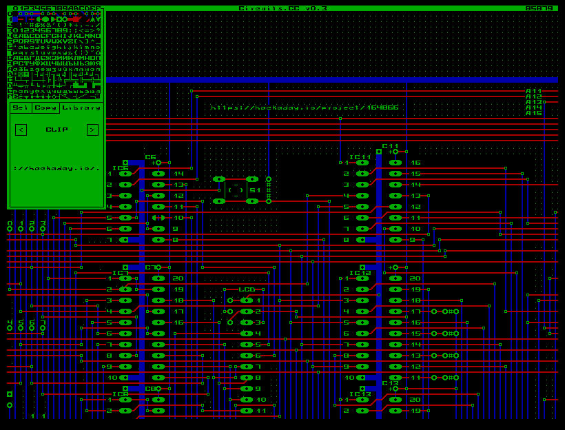
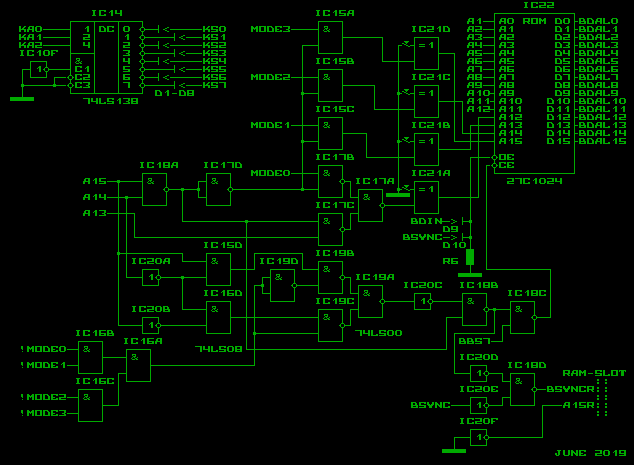
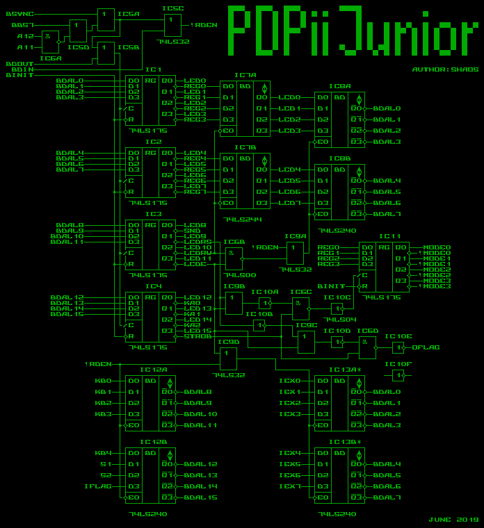
Also as part of this project I want to create an open source tool that will do auto-routing with Gerber output based on netlist. For now I do manual drawing in my own online multiuser PCB and schematics editor http://Circuits.CC :

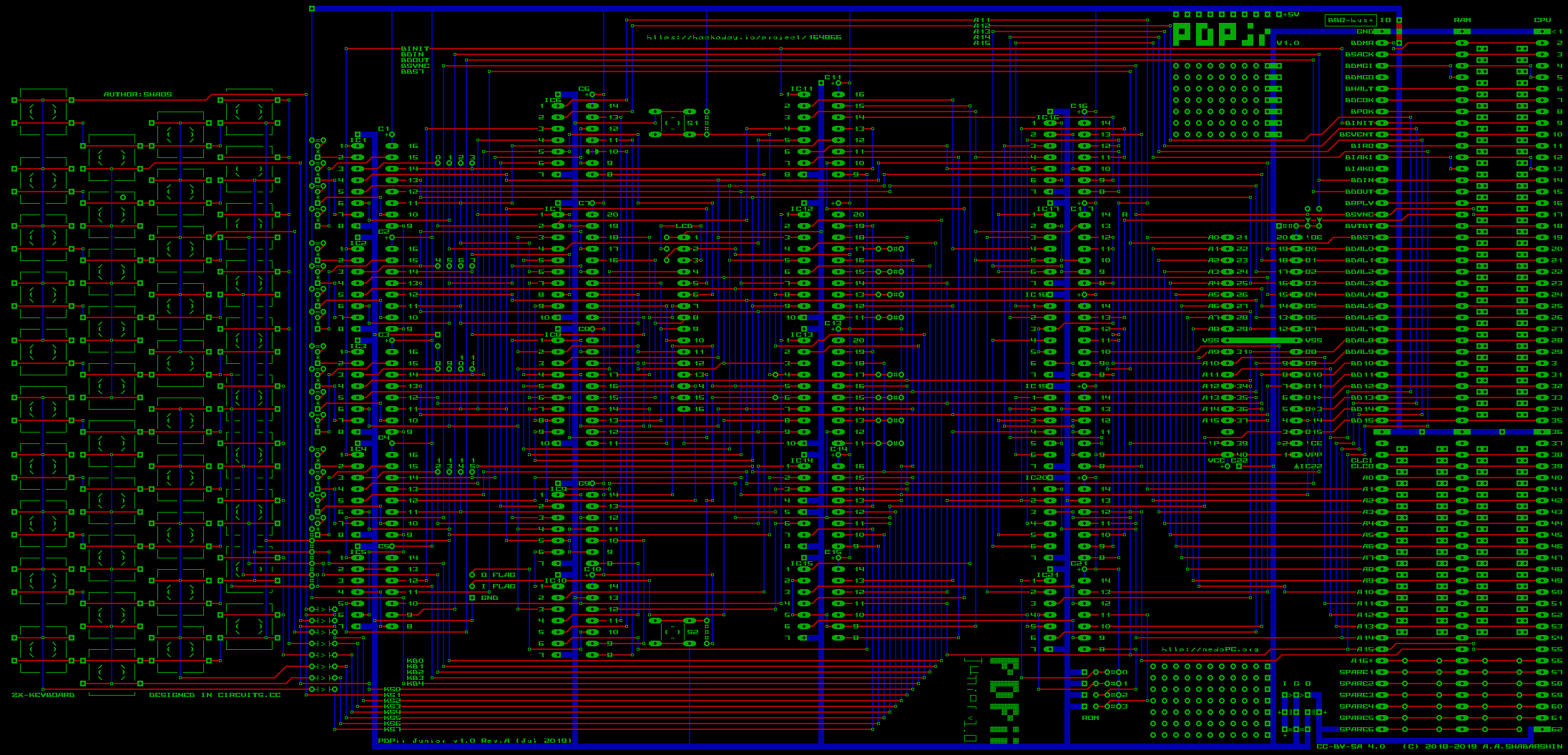
PCB dimensions are 6.6 x 13.7 inches:

Hackaday article (July 13, 2019):

https://hackaday.com/2019/07/13/a-pdp-laptop-for-various-definitions-of-a-laptop/

  • 1 × PDPjr motherboard Big one ;)
  • 1 × nedoPC-18.02 CPU module from PDPii project
  • 1 × nedoPC-18.20 RAM module from PDPii project

  • Board

    SHAOS07/13/2019 at 20:47 4 comments

    Finished main board design - it's 13.7 x 6.6 inches:

    For the board I used the same Circuits.CC (my online tool for making simple schematics and PCB):

    To make board image more readable I rotated it, moved to grayscale and inverted:

    and even printed in scale (160 dpi) to see if components are fitting well ;)

    Now I need to write C-program to convert my tiled pseudo-ASCII design to Gerbers for production ;)

    P.S. Just noticed a few things to fix - probably 1st of all I need to write C-program that is looking for errors like interrupted wires. incomplete pads etc...

  • Last piece of the puzzle

    SHAOS06/29/2019 at 06:45 0 comments

    Final part of the logic plus ROM:

    Here you can see how I do address bits manipulation for ROM to have memory models described earlier - now total count of integrated circuits is 22 (plus #PDPii CPU module and #PDPii RAM module). As I said before RAM module will have its own slightly modified BBQ-slot - instead of A15 it will have always "1" and custom BSYNC signal will be used to mask RAM in places where it's not supposed to be located. Also XOR chip IC21 will be used to mix ROM pages (just to be able to boot from any of them).

  • More TTL gates

    SHAOS06/28/2019 at 05:19 3 comments

    Now it looks much closer to completion:

    IC11 is bank register, that store 4 bits when LCDE=0, LCDRS=0 and STROB=1 for a short period of time and it's cleaned on boot (when BINIT=0). If LCDE=0 and LCDRS=1 then STROB goes out as OFLAG (will be used in future). Higher byte of the word is always going back to the BBQ-bus when !RDEN is 0 (Q-bus read cycle from address 0xF800...0xFFFE), but lower byte can be LCD data output if !RDEN=0, LCDE=1 and LCDRW=1 (read from LCD) or IEX0...IEX7 if !RDEN=0 and LCDE=0 (LCD disabled). Those 8 extra inputs are reserved for future so if it's not used then IC13 could be omited. REG0...REG7 are connected to LCD data bus only when LCDRW=0 (write to LCD).

    Next I should add ROM 27C1024 and show how to mix RAM module and ROM address signals with some logic to get memory modes described earlier - TO BE CONTINUED

  • Control register

    SHAOS06/27/2019 at 05:57 0 comments

    This is how it could be implemented (drawn in my Circuits.CC online editor):

    As you can see it writes data to register at the end of BDOUT=0 and BSYNC=0 (Q-bus write cycle) when BBS7=0 (it means A15=A14=A13=1) and A11=A12=1 (so technically speaking it will respond on any address from 0xF800 to 0xFFFE, but for future compatibility we are saying that address must be 0xFF00). We will use inverted outputs (REG0...REG15) to fix our inverted data bus and straight outputs will go to 16 LEDs for indication. Also BINIT signal will clean the register on boot (but because we use inverted outputs we will get value 0xFFFF). And finally we have signal !RDEN (read enabled) to connect buffer to databus when CPU reads (BDIN=0 and BSYNC=0 that is Q-bus read cycle) from address 0xFF00 (actual buffer schematics will be added later).


    TO BE CONTINUED

  • Memory map

    SHAOS06/24/2019 at 01:47 1 comment

    Original #PDPii memory modules occupy these address ranges:

    • nedoPC-18.10 aka "ROM module 64KWord or 128KB" - 0x0000...0x7FFF or 0x0000...0xFFFF (paging with jumpers);
    • nedoPC-18.20 aka "RAM module 32KB" - 0x8000...0xDFFF or 0x8000...0xFFFF (use or ignore /BBS7).

    Here I will not use ROM module, because ROM chip 27C1024 will be on motherboard itself with programmable paging (16 pages ROM0...ROM15 8KB each). RAM module will be inserted into dedicated BBQ-slot and split to RAM0 and RAM1 halves (16KB each) that will be connected to memory windows independently with help of some additional logic. So I plan to have 3 BBQ-sockets on that motherboard:

    • BBQ-bus+ socket for CPU module;
    • BBQ-bus+ socket for RAM module (this socket will be customized BBQ-socket just for RAM);
    • BBQ-bus+ socket for any I/O module controllable by /BBS7 signal (for example RC2014 adapter).

    Also motherboard will have 16-bit register (probably better to take 4 x 74LS175 to have ability to use inverted bits and clear it on RESET) and 16-bit buffer (inverting 2 x 74LS240) to write/read LCD accessible by address 0xFF00 (or 0177400 in octal system that was "native" for PDP-11). For keyboard addressing it will be 74LS138 decoder chip that converts 3-bit address to 8 control lines (and we will read 5 signals back from keyboard - similar to classic ZX-Spectrum):

    For bank switching we can take 4-bit register and make it accessible with some combination of control bits when LCD is disabled. That bank switching latch will encode memory mode:

    Memory
    mode

    Window 0
    0x000...0x3FFF
    Window 1
    0x4000...0x7FFF
    Window 2
    0x8000...0xBFFF
    1st half of Win3
    0xC000...0xDFFF
    0000ROM0 + ROM1
    RAM1RAM0ROM0
    0001RAM0RAM1ROM0 + ROM1
    ROM1
    0010RAM0RAM1ROM0 + ROM1ROM2
    0011RAM0RAM1ROM0 + ROM1ROM3
    0100RAM0RAM1ROM0 + ROM1ROM4
    0101RAM0RAM1ROM0 + ROM1ROM5
    0110RAM0RAM1ROM0 + ROM1ROM6
    0111RAM0RAM1ROM0 + ROM1ROM7
    1000RAM0RAM1ROM0 + ROM1ROM8
    1001RAM0RAM1ROM0 + ROM1ROM9
    1010RAM0RAM1ROM0 + ROM1ROM10
    1011RAM0RAM1ROM0 + ROM1ROM11
    1100RAM0RAM1ROM0 + ROM1ROM12
    1101RAM0RAM1ROM0 + ROM1ROM13
    1110RAM0RAM1ROM0 + ROM1ROM14
    1111RAM0RAM1ROM0 + ROM1ROM15

    On reset it will be memory mode 0000 (ROM in window 0 then RAM1 then RAM0) then BIOS will programmatically switch memory mode to something else to have RAM in the 1st half of memory to be able to run RT-11 apps and 1st half of Window 3 will be used to access other ROM pages. 2nd half of Window 3 will always be BBS7 area for peripheral devices inserted into 3rd slot. Also it is possible to add 4 jumper switches to mix ROM pages to start from any ROM page if needed (for debug purposes for example).


    Description of every bit of memory location 0xFF00 (LCD control register and keyboard reading):

    BitOn write
    On read
    0LCD data bit 0 (also goes to bank register)
    LCD data bit 0
    1
    LCD data bit 1 (also goes to bank register)LCD data bit 1
    2LCD data bit 2 (also goes to bank register)
    LCD data bit 2
    3LCD data bit 3 (also goes to bank register)
    LCD data bit 3
    4LCD data bit 4LCD data bit 4
    5LCD data bit 5LCD data bit 5
    6LCD data bit 6LCD data bit 6
    7LCD data bit 7LCD data bit 7
    8LED output (error) and may be sound (?)
    Keyboard data bit KB0
    9LCD control input RS (0 - command, 1 - data)
    Keyboard data bit KB1
    10LCD control input R/W (0 - write, 1 - read)
    Keyboard data bit KB2
    11LCD control input E (0 - disable LCD, 1 - enable LCD)
    Keyboard data bit KB3
    12Keyboard address bit KA0
    Keyboard data bit KB4
    13Keyboard address bit KA1
    Extra button S1 (?)
    14Keyboard address bit KA2
    Extra button S2 (?)
    15Extra output (goes to bank register if E=0 and RS=0)
    Extra input (reserved for future use)

View all 5 project logs

Enjoy this project?

Share

Discussions

Similar Projects

Does this project spark your interest?

Become a member to follow this project and never miss any updates