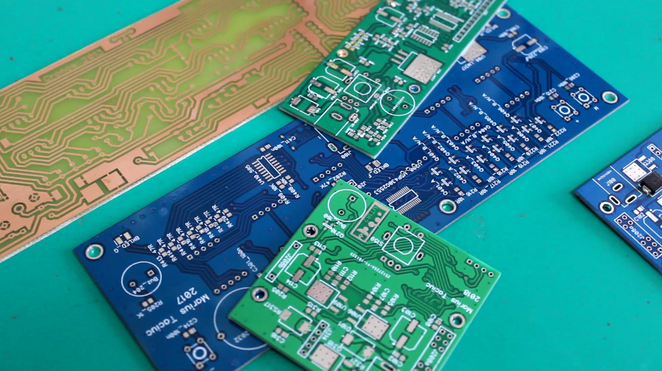
Of course, this method of photo etching was having it's drawbacks like I couldn't make double sided PCB, I had to add wires to the other side or to keep it into an intelligent shape and reroute the traces between the pads in the most efficient way.
during my pioneering years, back in 1997, i really didn't have access to software designing tools like the modern available ones. Now I'm using the latest version of LTspice and DipTrace to create and test my schematics. And of course, Dip trace also has the layout module which allows you to create your boards for free. Back then, the best method was to place the components on a paper covered styrofoam board and then copy the drawing to a copper laminate. I made my own ink from some bitumen solved into some paint solvent. I was then drawing the traces by hand using a pen and manually etching them using ferric chloride, nitric acid or hydrochloric acid with perhydrol. Of course this was very time consuming, the quality was low and I was very limited in what comes the number of traces per cm, the package of the components and the spacing.
After I moved on with the photo etching method, the things improved as I could suddenly use surface mount components, thinner traces (of 0.5 - 1 mm). But his wasn't good enough. I definitely needed a fast way of creating double sided PCB and the possibility of adding viases to the board.
Then I discovered some online websites which are providing prototyping for PCBs at lower prices. One of them is JLCPCB.com
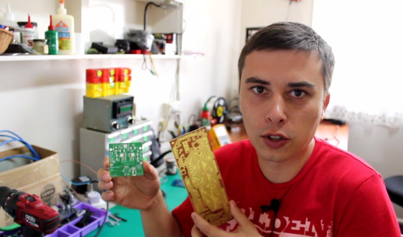
 Marius Taciuc


 Michael Delaney
 PCB designer
 alongruss
 Lithium ION
By the way I use EasyEDA (JLCPCB) and are pretty happy with them.
Not foolproof but fast delivery.
Minimum order is 5 boards (so a lot of wastage).
The boards are okay but you are likely to damage the board if you try to remove components.
Do check the design manager for errors, carefully.
When using third party component designs, do check for errors like incorrect pin numbers.
Be careful not to mis-number your ICs, it may not trip an error.
Due to updates, old designs may not autoroute (the components may have changed).
Finally, the online autorouter is usually unavailable (too busy) so you need to download and run the local autorouter. The autorouter is pretty good but some designs are just too hard for it to solve.
So I would give then 7/10.
AlanX