This is the current state of the ALU design. There are still several loose ends. Carry signals for addition and shifting are not yet present. The ALU is 8 bits wide, but for clarity I only show 4 bits. (Clicking it will show a better readable version).
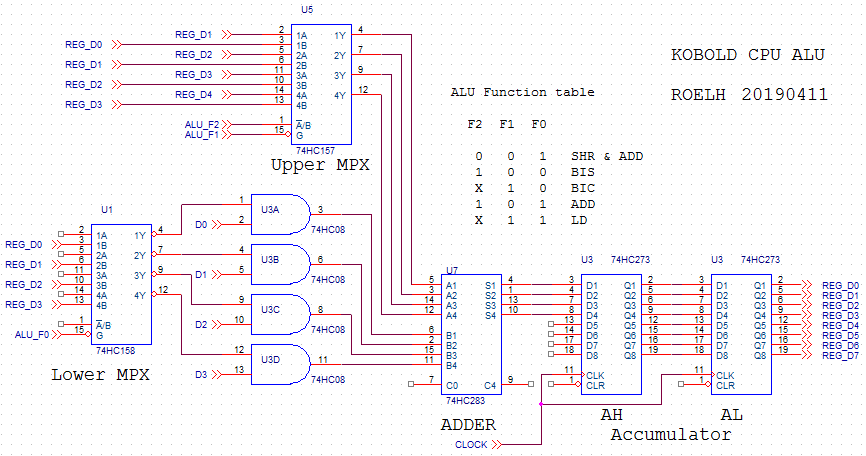
The ALU functions are LOAD, ADD, BIS, BIC, SHR and SHL
The ALU is intended to work on 16 bit words, in two sequential cycles that each handle a byte.
ADD function
The ADD function is the easiest to explain. The upper MPX (multiplexer) connects the output of the AL accumulator byte to the upper inputs of the adder chip, 74HC283. The lower MPX is disabled (by ALU_F0 signal), so all its outputs are high. That means that the input from the databus (D0-D7) is flowing through the AND-gates to the lower inputs of the adder chip. So, the adder will add the databus byte to the AL byte and deliver the result in AH.
Ooops... what is that lower byte doing in the high part of the accumulator ? And the accumulator has been clocked, so the high byte of the accumulator is now in the low byte ?
After the next cycle, it will be all right. The high byte coming from the databus will be added to the high byte of the accumulator, that is in AL now. The result will go to the AH register, and the previous result of the low byte will at the same time go to the AL register.
LOAD function
How do we put something in the accumulator ? We set the ALU-F1 signal (connected to the upper MPX) to 1. This disables the upper MPX, its output will be zero. We now do the ADD operation. The databus contents will be added to zero, and the result will be put in the accumulator.
BIC function
For the BIC (bit clear) function (that is a logical AND where one of the operands is inverted), the upper MPX is disabled but the lower MPX is now enabled. The lower MPX inverts the data (it is a 74HC158). The following AND gates will give result: DATA and (not ACCU). The adder will add zero to this, so that does not change the result. So the result is that any bit that was set in the accumulator, will cause the same bit from the databus input to be cleared.
BIS function
The BIS (bit set) function (PDP11 parlance for logical OR) is similar to BIC, but now also the upper MPX is enabled again. so both adder inputs can receive data. When an accumulator bit is 0, the AND gates will transfer the databus inputs, the adder will add the 0 bit to it, so result for this bit is 1 (if there was no carry from previous bit). And when an accumulator bit is 1, it is inverted by the lower MPX so it delivers 0 to its AND gate, so the lower input of the adder will be 0. The adder output will be 1 because the upper input is 1 and the lower input is 0. The key idea is, that at the adder, the two inputs for a certain bit are never both 1. In this case, the adder will never generate an (internal or external) carry, and will behave as four OR gates.
SHR function
Finally, the SHR (shift right) function can be done by the upper MPX, because it has a shifted version of the accumulator bits connected to one of its input groups. The databus input should be zero (or not, in that case it will be added to the result).
SHL function
SHL (shift left) is the same as adding.
Other functions
A few functions are missing, but they can be composed from the functions that are available. This can be done in microcode, so the instruction set can still contain these missing functions. It will only have a small impact on performance. The functions that I'm talking about are SUB, XOR and NOT.
[edit: ALU design changed due to switching to 16 bit design, new version is here]
Discussions
Become a Hackaday.io Member
Create an account to leave a comment. Already have an account? Log In.