 Sonny Lloyd
“Shoot-through” is the name given to a failure event when two adjacent switches in a voltage source inverter are ON simultaneously thus short-circuiting the supply, as shown in Figure 1. This failure mode can easily become catastrophic especially in motor drive application where the DC link capacity is rather large and has more than enough stored energy to cause a fire if the shoot-through event is not extinguished within a very short time, typically 10µs for a rugged IGBT (other switch technology can be more sensitive and require even faster response times).
Figure 1: Shoot-through Event
It is interesting to note that the vast majority of the short-circuit current does not come from the traction battery back but rather the inverter’s DC link capacitor which has a very low impedance path between it and the power switches. This means that any current sensor between traction pack and the capacitor will not “see” the fault current and therefore cannot detect the fault. In fact, since there are no current sensors at all in the short-circuit path it makes detecting this type of fault challenging.
To detect a shoot-through event the gate driver (external to Axiom control board) employs a power switch “desaturation detection” circuit. The gate driver will immediately shut down the local IGBT when a desat fault is detected. When this first IGBT is shutdown the high fault current is extinguished before it becomes catastrophic and the Axiom control board will be notified so that its firmware can work to immediately shut down the other five switches, thus disabling the drive completely. Desaturation detection is a simple circuit, but its simplicity can often be mistaken for simple to design. The circuit must be 100% reliable in a high noise environment, be extremely fast acting and sufficiently stable over a very wide temperature range. Each component in a desaturation detection circuit is carefully considered and the PCB layout is similarly critically analyzed.
Now that the shoot-through event has been summarized, along with detection and shut down method, the next question is why would a shoot-through event even happen in the first place? Surely the control scheme is such that the processor would never issue ‘ON’ command simultaneously to two adjacent switches. No doubt this is the case.. but for unproven firmware, with well over 100,000 lines of code, its possible that a firmware bug may exist .. and its possible that such a bug could lead to errant command signals. More likely however is that noise from high voltage and high current switching gets coupled back into the control board causing unpredictable erratic behaviour, including causing a shoot-through.
Since the shoot-through event has the capability to be destructive it is well worth the designers time to invest an effort to prevent, however possible, the mis-firing of PWM signals. Axiom accomplishes this goal in several ways. The microcontroller firmware is based on proven code, used by thousands of users in a wide variety of applications. Despite this, Axiom makes use of an FPGA which monitors the IGBT gating commands to ensure, double ensure that the microcontroller does not issue errant PWM signals.
Figure 2: Overlap Protection Logic Circuit
The idea of this circuit is to allow the microcontroller to turn on its associated gate driver, either the top or the bottom, but never the top and the bottom simultaneously (shoot-through!).
The logic truth table is deciphered as:
Figure 3: Overlap Protection Logic Circuit Truth Table
In earlier revisions of Axiom the PWM overlap protection circuit really was implemented like this using discrete hardware. More recently the simplistic logic diagram is implemented in an FPGA (see previous log HERE)
Once the PWM has been checked by the overlap protection logic, it heads off to the Gate Driver board whose job is to turn digital PWM into a power pulsed equivalent to drive the IGBT. The Gate Driver board sits right at the interface between noise high power IGBT and sensitive digital and therefore becomes the most critical component to overall function. Members of EV Power Designs have been designing Gate Driver boards for high performance application for over 15 years, a version of which went into a World Record Breaking race down the 1/4 mile track. Hard experience has taught that a rock solid, highly fault tolerant, excellent common-mode rejection capability, desaturation detection, two-step turn OFF and other built in features are required for high power high performance motor drive application. Besides our own custom design which have these features, EV Power Designs also recommends gate drivers by Power Integrations (formally IGBT-Concepts).
With digital voltage on one side, high switching voltage on the other and a dielectric in between (plastic case of the opto-isolator) suddenly you have an effective capacitor injecting noise current through it (from switching high voltage gate driver to digital, noise current crawling over the plastic case. For lower power applications this is practically a non-issue, but high power its a real concern. Not all opto-coupler, gate drive IC’s or PCB layouts are up to the challenge. This concept, also applies to the gate driver power supply, specifically the transformer. Noise can travel through the parasitic capacitance here too, so less than 5pF input-to-output capacitance is desired.
Is the story done? There’s still one more major failure mode to be considered. It was previously mentioned the shoot-through current is extremely high and lasts only a short period of time (desat protection opens the circuit in less than 10µs), but that time is enough to charge the stray inductance of the fault current path shown in Figure 1. This could be represented schematically by placing the inductor symbol for the DC link capacitor (internal inductance + connection to IGBT) and the internal inductance + connection of the IGBT itself.. both of them, like so:
Figure 4: Stray Inductance in Shoot-through Path
The high current flows through the stray inductance(es) and then the desat protection circuit opens one of the switches to protect the system. As is well known to Electrical Engineers, the current in an inductor wants to continue to flow and when an inductor is suddenly open circuited, a voltage will spike to very high values in an attempt to keep the current flowing. At the power levels typical to Axiom, the stored energy is significant and the voltage spike can be destructive. The irony of the situation, the desat protection circuit worked but it caused another problem! Therefore the system has to be designed to mitigate this potential hazard as well. EV Power Designs has three solutions to contain the voltage spike within tolerable limits. Firstly, the Axiom control board was intentionally designed to mount directly to a gate driver from Power Integration (formally IGBT-Concepts) which was specifically chosen for its rugged construction and reliable fault management and that direct mounts on a very stray low inductance IGBT from Infineon. Secondly, EV Power Designs contracted a capacitor manufacturer to specially design a DC Link capacitor with very low internal self inductance. Thirdly, the proposed connection between DC link capacitor and IGBT switch is maintained at absolute minimal length with no need for external copper busing or snubber capacitor.
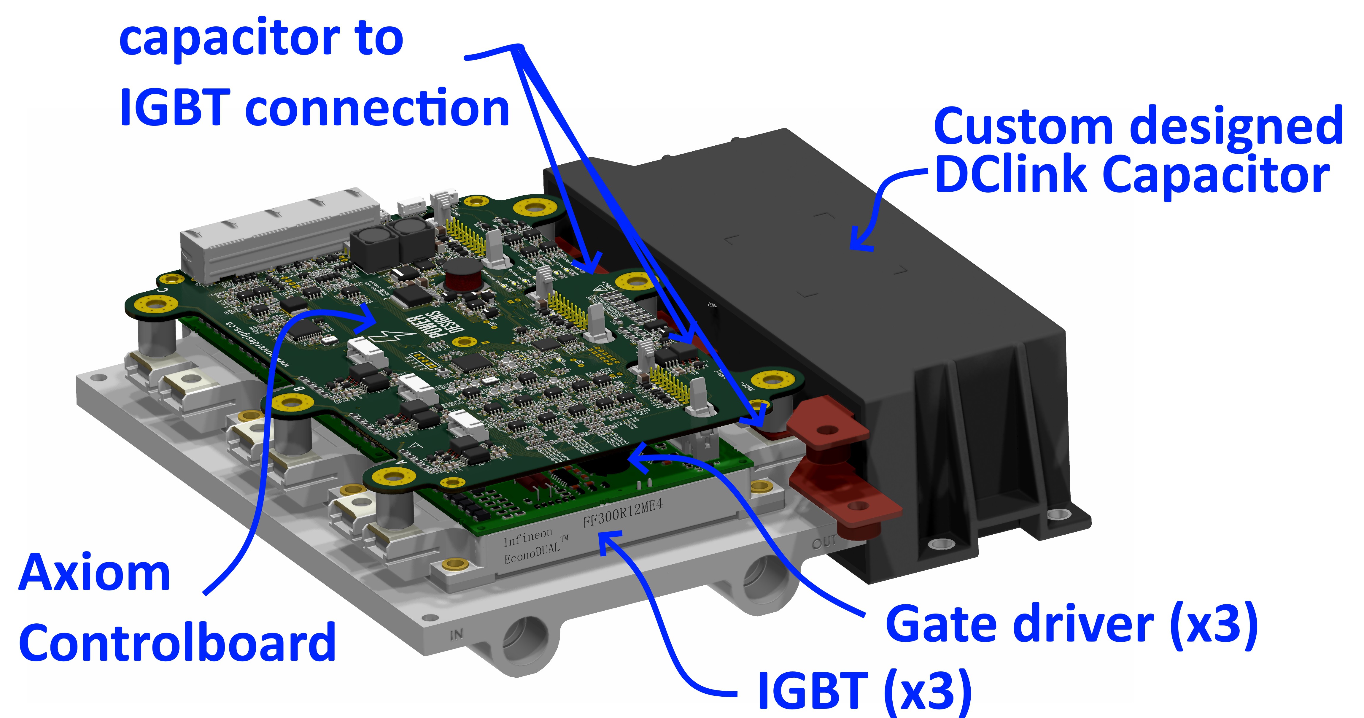
Figure 5: Full Up Controller Designed and Assembled for Minimal Stray Inductance
Multiple levels of protection have been designed into the motor drive full up controller to properly manage the threat of a shoot-through, or the voltage spike which occurs after a shoot-through event.
Deep Dive over, lets resurface shall we?
Discussions
Become a Hackaday.io Member
Create an account to leave a comment. Already have an account? Log In.